Electroluminescent device, method of manufacturing the device, electronic device, thin-film structure, and method of forming thin film

a technology of electroluminescent devices and thin films, which is applied in the direction of discharge tubes/lamp details, discharge tubes luminescent screens, coatings, etc., can solve the problems of inability to achieve the desired thickness of the final thin film layer, inability to achieve the desired thickness, and inability to eject thin film liquid to the adjacent pixel, etc., to achieve uniform thickness and higher fineness

Inactive Publication Date: 2008-10-02
SEIKO EPSON CORP
View PDF2 Cites 31 Cited by
  • Summary
  • Abstract
  • Description
  • Claims
  • Application Information

AI Technical Summary

Benefits of technology

[0012]An advantage of some aspects of the invention is that an electroluminescent device that can have a substantially uniform thickness can be provided, even if a thin-film layer having very small dimensions is formed for meet...

Problems solved by technology

However, the above-mentioned ink-jet system has a problem in its process.
However, in a case that a thin-film pattern is formed by ejecting a thin-film material liquid using an ink-jet system, there is a problem that the ejected thin-film material liquid penetrates to the adjacent pixel.
Consequently, imbalance between the volume of a droplet to be ejected to a region surrounded by a bank and the areas of the bank surface and the region surrounded by the bank causes the following problems.
That is, in a case that the bank has a lyophilicity or wettability to the thin-film material liquid to be filled with, the final thin-film layer cannot have a desired thickness, even if the bank is formed, because the liquid...

Method used


Image

  • Electroluminescent device, method of manufacturing the device, electronic device, thin-film structure, and method of forming thin film
  • Electroluminescent device, method of manufacturing the device, electronic device, thin-film structure, and method of forming thin film
  • Electroluminescent device, method of manufacturing the device, electronic device, thin-film structure, and method of forming thin film

Examples


Embodiment Construction

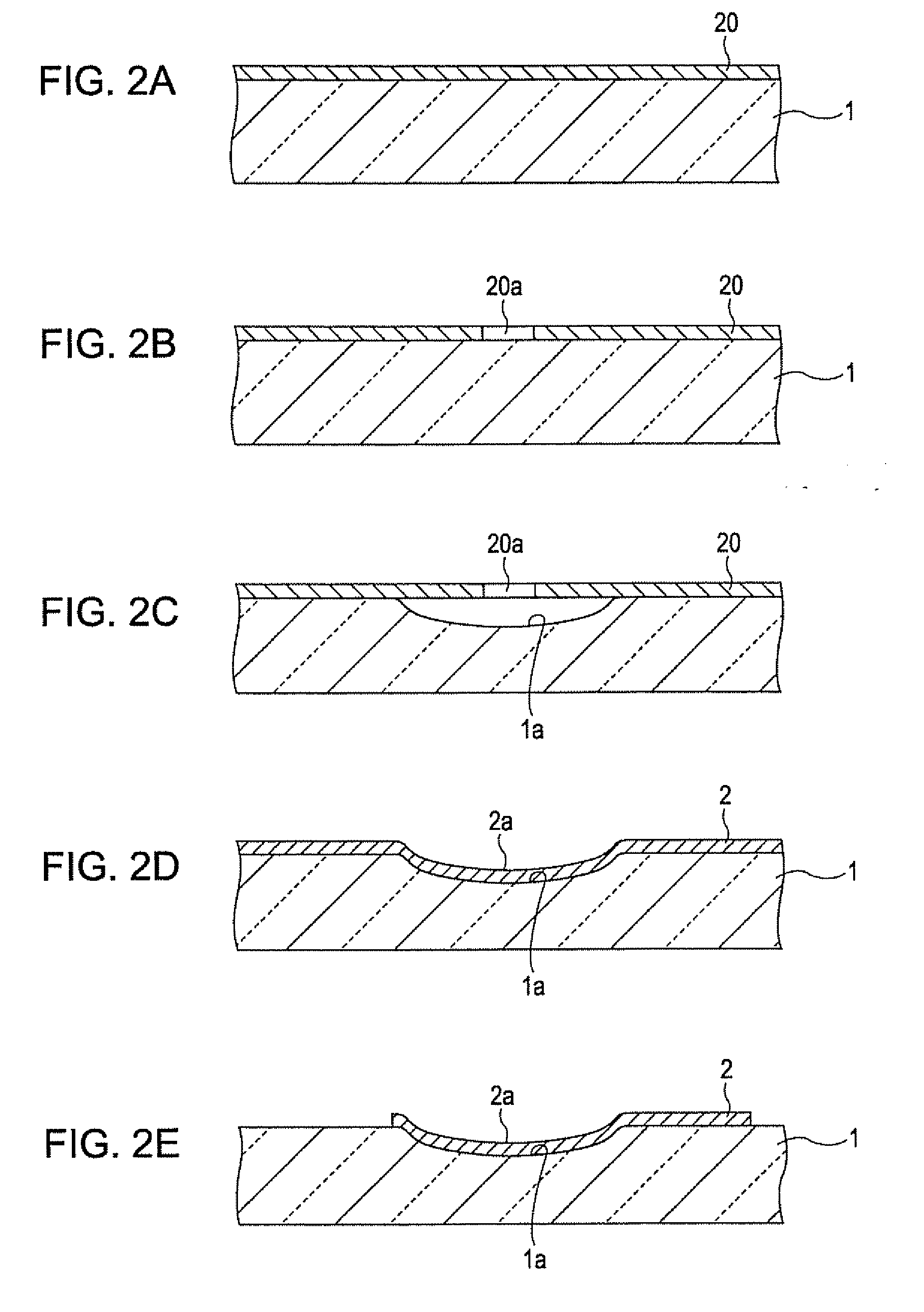
[0035]In accordance with embodiments of the invention, an electroluminescent device, a method of manufacturing the device, an electronic device including the electroluminescent device or an electroluminescent device manufactured by the method, a thin-film structure, and a method of manufacturing the thin film will be specifically described with reference to the accompanying figures.

Electroluminescent Device

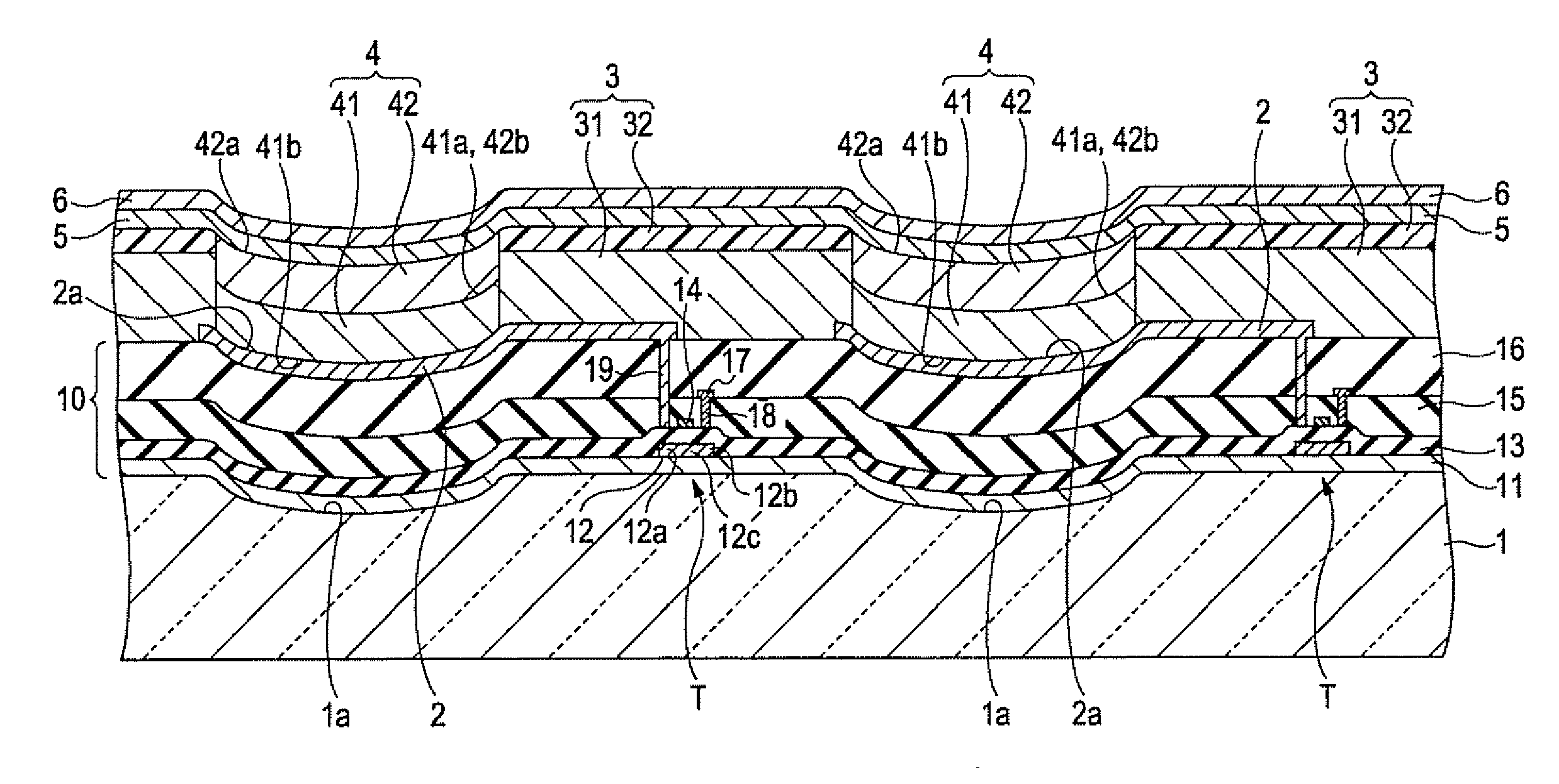
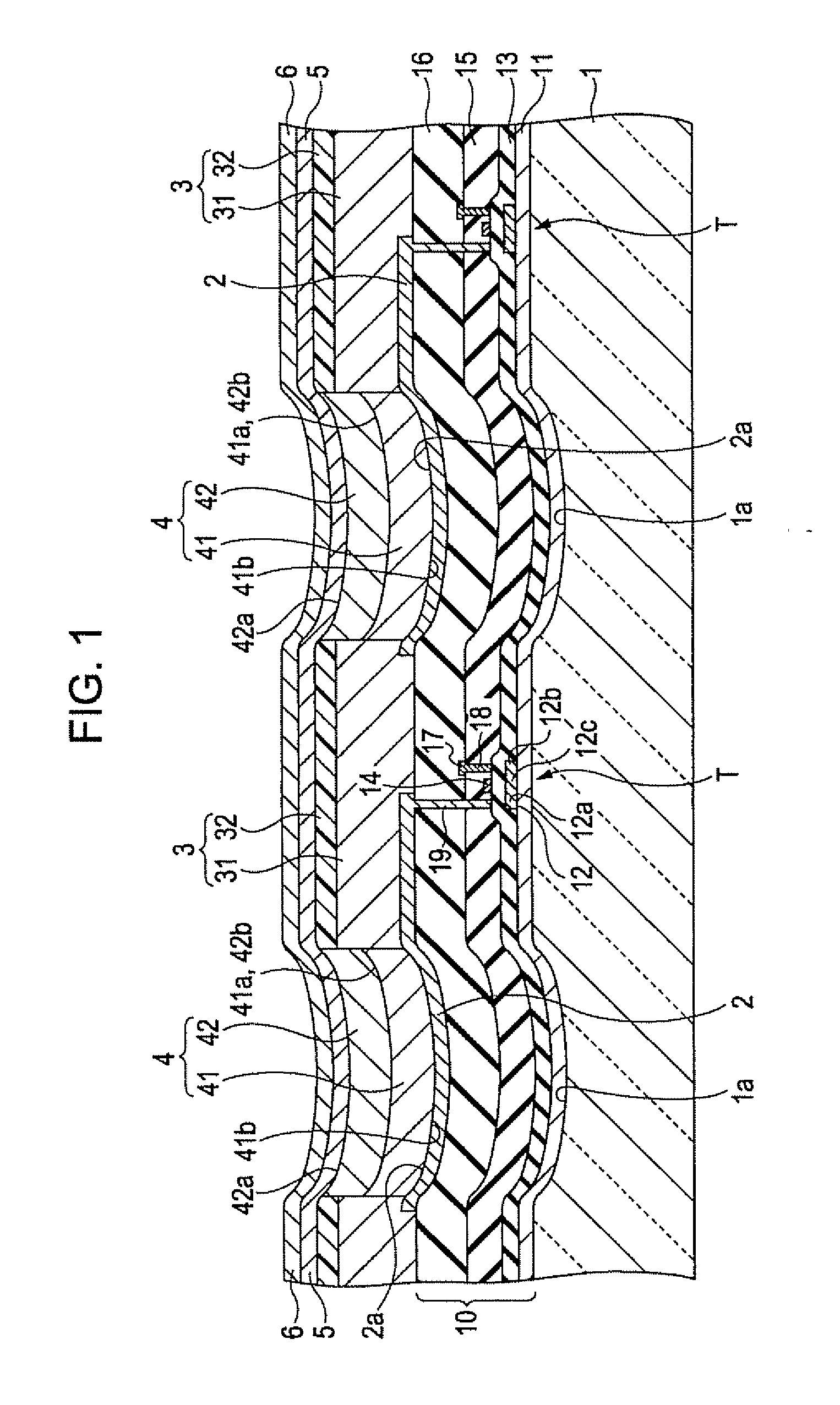
[0036]FIG. 1 is a longitudinal sectional view illustrating an electroluminescent device according to an embodiment of the invention. In this embodiment, the invention is applied to an organic EL device (organic EL emitting device) as the electroluminescent device. In particular, in the embodiment shown in the figure, the invention is applied to an active matrix organic EL device, and a thin-film transistor is used as the active element.

[0037]The organic EL device includes a substrate 1 made of glass or the like and a circuit element portion 10 having a thin-film transistor T on th...


PUM


Abstract

An electroluminescent device includes a substrate having a bank-forming face on one surface thereof, a bank formed on the bank-forming face, and a thin-film layer constituting an electroluminescent element at a region surrounded by the bank. The thin-film layer is formed by filling the region surrounded by the bank with a thin-film material liquid and solidifying the liquid. The bank-forming face and a contact face with the thin-film layer have curved surfaces so that the central portions thereof are convexed toward the substrate side.

Description

BACKGROUND[0001]1. Technical Field[0002]The present invention relates to an electroluminescent device including an electroluminescent element such as an EL (electroluminescent) element using an organic semiconductor film or an LED (light-emitting diode) element and relates to a method of manufacturing the electroluminescent device. The invention further relates to an electronic device including the electroluminescent device, a thin-film structure, and a method of manufacturing a thin film.[0003]2. Related Art[0004]In manufacturing of EL elements, color filters, and so on, technology for obtaining functional elements have been developed. In such technologies, thin-film layers that are independent of each other or have different characteristics are formed on a single substrate by coating or the like so as to have a predetermined pattern. In one effective method, for example, different thin-film patterns are formed on a single substrate using an ink-jet system.[0005]However, the above-...

Claims


Application Information

Patent Timeline
IPC IPC(8): H01J1/62B05D5/12
CPCH01L27/3246H01L51/0003H01L51/52H10K59/122H10K71/12H10K50/80
Inventor TAKEI, SHUICHICHINO, YUJI
Owner SEIKO EPSON CORP
Why Eureka
Try Eureka