

Capacitor built-in wiring board
a technology of built-in wiring and capacitors, which is applied in the direction of stacked capacitors, fixed capacitor details, thin/thick film capacitors, etc., can solve the problems of affecting the mcm tends to crack or a faulty connection can not be repaired, and the capacitor cannot be formed. , to achieve the effect of improving the reliability of the wiring board, increasing the capacity of the capacitor, and reducing mechanical stress
- Summary
- Abstract
- Description
- Claims
- Application Information
AI Technical Summary
Benefits of technology
Problems solved by technology
Method used
Image

Examples
first embodiment
[0075]Hereafter, a first embodiment for carrying out a capacitor built-in wiring board according to the present invention will be described in detail with reference to the drawings.
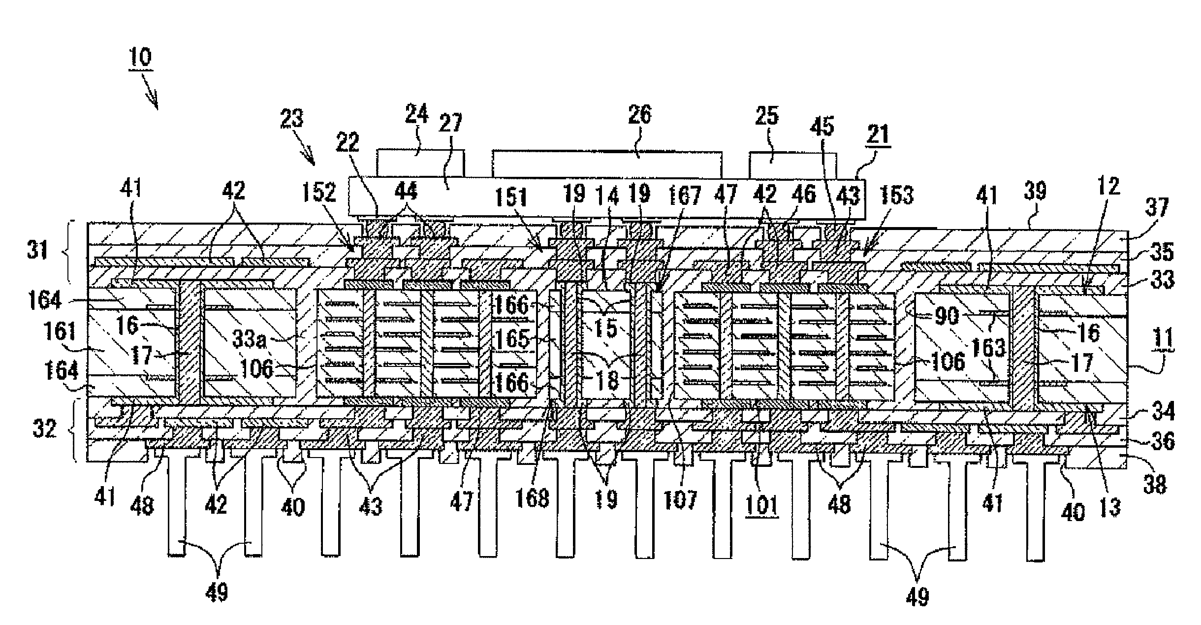
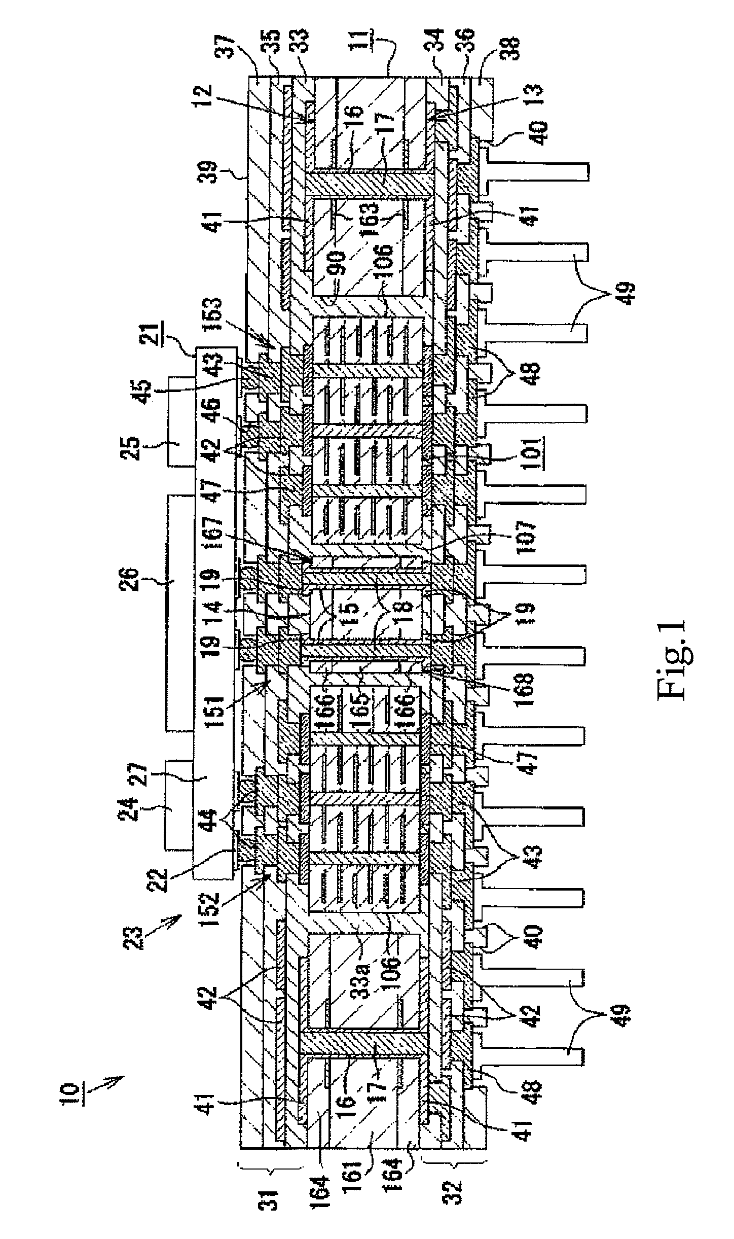
[0076]As shown in FIG. 1, a capacitor built-in wiring board 10 (hereinafter referred to as a “wiring board”) in accordance with the first embodiment is a wiring board for mounting an electronic component, and comprising: a core board 11 assuming a generally rectangular shape, a first buildup layer 31 (laminated wiring portion) formed on a core main surface 12 (upper surface in FIG. 1) of the core board 11 and a second buildup layer 32 formed on a core rear surface 13 (lower surface in FIG. 1) of the core board 11.
[0077]The first buildup layer 31 formed on the core main surface 12 of the core board 11 has a structure in which two resin insulating layers 33 and 35 (hereinafter referred to as an interlayer insulating layer) made of thermosetting resin (epoxy resin) and a conductor layer 42 made of copper are...
second embodiment
[0131]Next, a second embodiment for carrying out a capacitor built-in wiring board according to the present invention will be described in detail with reference to the drawings. In the following description, same explanations as those of the wiring board 10 will be omitted, and only point differently from those of the wiring board 10 will be explained.
[0132]As shown in FIGS. 22, 23 and 24, a conductor containing portion 14′ is formed in the center of a core board 11′. The conductor containing portion 14′ according to the second embodiment has a generally square shape as seen from the plane view with the size of 3.0 mm long×3.0 mm wide×1.0 mm thick. The conductor containing portion 14′ is a part of the core board 11′ and is comprised of a part of the substrate 161 and a part of the sub-substrate 164. Further, the conductor containing portion 14′ includes a plurality of copper-made current supplying conductors 15 (four in the second embodiment) is formed so as to penetrated the core m...
PUM
 Abstract
Description
Claims
Application Information