Method of manufacturing semiconductor laser, semiconductor laser, optical pickup, optical disk device, method of manufacturing semiconductor device, semiconductor device, and method of growing nitride type group iii-v compound semiconductor layer

Active Publication Date: 2008-10-02
SONY CORP
View PDF2 Cites 17 Cited by
  • Summary
  • Abstract
  • Description
  • Claims
  • Application Information

AI Technical Summary

Benefits of technology

[0049]According to the present embodiment, it is possible to realize a semiconductor laser using a nitride type Group III-V compound semiconductor wherein an end face window structure can be formed extremely easily, the optical waveguide loss can be suppressed, and it is possible to prevent light absorption or local heat generation from occurring at the time of laser operation. With the

Problems solved by technology

As above-mentioned, the methods for forming the end face window structure in a semiconductor l

Method used


Image

  • Method of manufacturing semiconductor laser, semiconductor laser, optical pickup, optical disk device, method of manufacturing semiconductor device, semiconductor device, and method of growing nitride type group iii-v compound semiconductor layer
  • Method of manufacturing semiconductor laser, semiconductor laser, optical pickup, optical disk device, method of manufacturing semiconductor device, semiconductor device, and method of growing nitride type group iii-v compound semiconductor layer
  • Method of manufacturing semiconductor laser, semiconductor laser, optical pickup, optical disk device, method of manufacturing semiconductor device, semiconductor device, and method of growing nitride type group iii-v compound semiconductor layer

Examples


first embodiment

[0094]FIGS. 8 to 29 illustrate the method of manufacturing a GaN semiconductor laser according to the present invention. The GaN semiconductor laser has an end face window structure and a ridge stripe structure, wherein parts, in the vicinity of resonator end faces, of a p-side electrode are removed so that both end parts of the resonator are set as current non-injection region.

[0095]In the first embodiment, first, as shown in FIG. 8 and FIGS. 9A and 9B, a chip region 12 as a region to finally be one laser chip is defined on an n-type GaN substrate 11. Then, in the chip region 12, insulating film masks 16 having a trapezoidal plan-view shape are formed in the vicinity of resonator end face forming positions 13, 14, where front-side and rear-side resonator end faces are to be finally formed by cleavage or the like, and on both sides of a ridge stripe forming position 15 where a ridge stripe is to be formed later, in line symmetry with respect to the ridge stripe forming position 15. ...

second embodiment

[0132]Now, a method of manufacturing a GaN semiconductor laser according to the present invention will be described below.

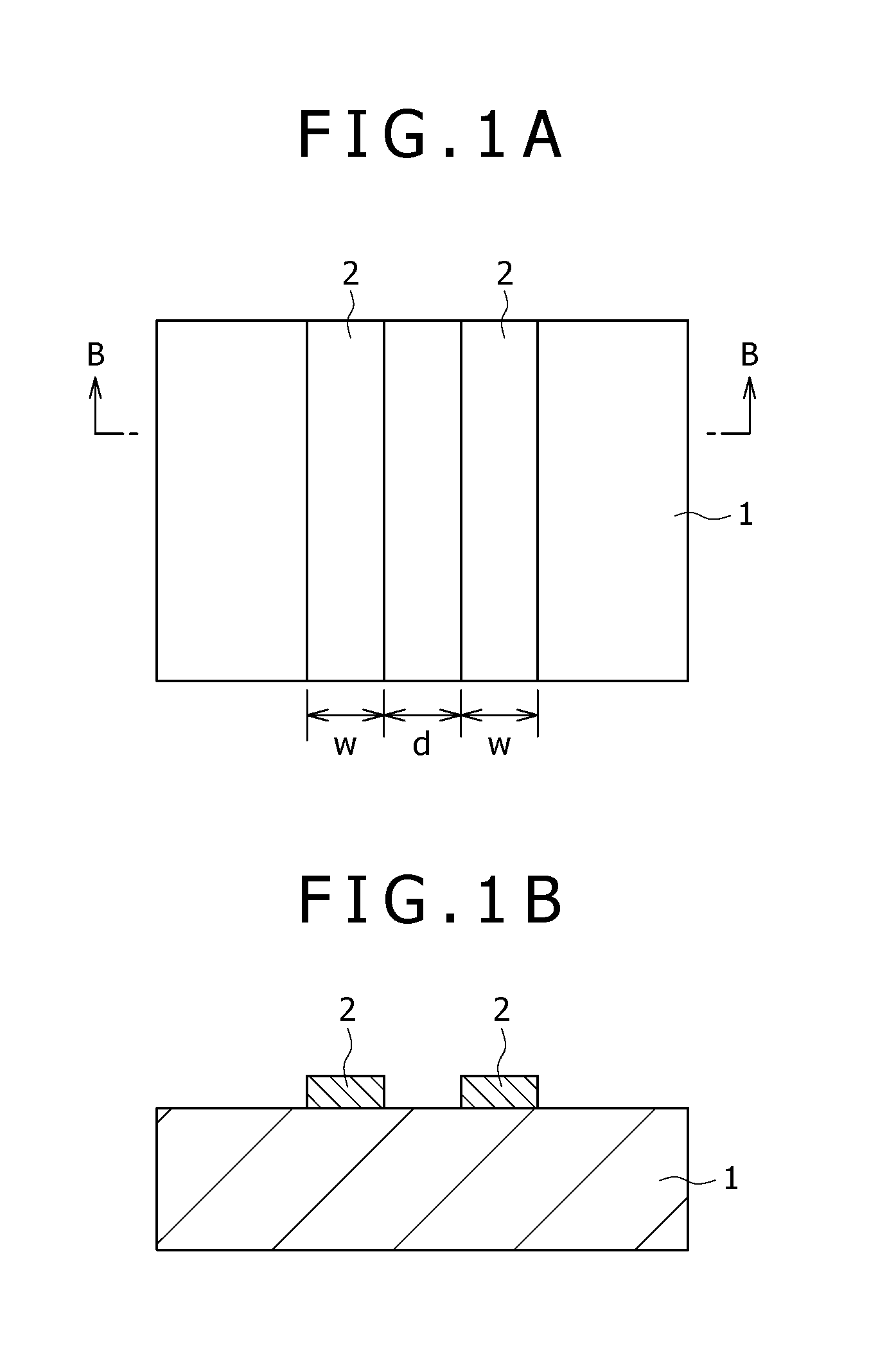
[0133]In the second embodiment, first, as shown in FIG. 30, an elongate insulating film mask 16 with a fixed width is formed on a n-type GaN substrate 11 on one side of the ridge stripe forming position 15 and along the whole length of the resonator in the resonator length direction. One edge of the insulating film mask 16 on the ridge stripe forming position 15 side is coinciding with one edge of the ridge stripe forming position 15, in its central portion in the resonator length direction. However, in its portion within a distance d1 from each of the resonator end face forming position 13, 14, the one edge of the insulating film mask 16 is spaced from the ridge stripe forming position 15 by a spacing w1, and, in the portion at a distance d1 to d2 from each of the resonator end face forming positions 13, 14, the spacing is gradually reduced from w1 to 0. One non...

third embodiment

[0137]Now, a method of manufacturing a GaN semiconductor laser according to the present invention will be described below.

[0138]In the third embodiment, first, as shown in FIG. 31, the insulating film mask 16 used in the second embodiment is formed on the n-type GaN substrate 11 on each of both sides of the ridge stripe forming position 15, in line symmetry. One non-limitative example of the dimensions is such that d1 is 20 μm, d2 is 50 μm, the width of the insulating film mask 16 is 5 μm, and the spacing w1 between the insulating film mask 16 and the ridge stripe forming position 15 is 3 to 20 μm.

[0139]Next, in the same manner as in the first embodiment, the GaN semiconductor layer 25 is grown on the n-type GaN substrate 11 (provided with the insulating film masks 16) by the MOCVD method, for example. In this case, as for the active layer 19 containing In and Ga, in the area between the pair of the insulating film masks 16 in the portions within a distance d2 from the resonator end...


PUM


Abstract

A method of manufacturing a semiconductor laser having an end face window structure, by growing over a substrate a nitride type Group III-V compound semiconductor layer including an active layer including a nitride type Group III-V compound semiconductor containing at least In and Ga, the method includes the steps of: forming a mask including an insulating film over the substrate, at least in the vicinity of the position of forming the end face window structure; and growing the nitride type Group III-V compound semiconductor layer including the active layer over a part, not covered with the mask, of the substrate.

Description

CROSS REFERENCES TO RELATED APPLICATIONS[0001]The present invention contains subject matter related to Japanese Patent Application JP 2007-050461 filed with the Japan Patent Office on Feb. 28, 2007, the entire contents of which being incorporated herein by reference.BACKGROUND OF THE INVENTION[0002]1. Field of the Invention[0003]The present invention relates to a method of manufacturing a semiconductor laser, a semiconductor laser, an optical pickup, an optical disk device, a method of manufacturing a semiconductor device, and a method of growing a nitride type Group III-V compound semiconductor layer, and is preferable when applied, for example, to a ridge stripe type semiconductor laser having an end face window structure using a nitride type Group III-V compound semiconductor, and an optical pickup and an optical disk device which use the semiconductor laser as or in a light source.[0004]2. Description of the Related Art[0005]In order to increase the maximum optical output of a s...

Claims


Application Information

Patent Timeline
IPC IPC(8): H01S5/22H01L33/00H01S5/343
CPCB82Y20/00G11B7/125H01S5/106H01S5/34333H01S5/164H01S5/2077H01S5/2272H01S5/1064
Inventor KURAMOTO, MASARUNAKAYAMA, EIJIOOIZUMI, YOSHITSUGU
Owner SONY CORP
Why Eureka
Try Eureka