Apparatus and method for predictive temperature correction during thermal processing

a technology of thermal processing and apparatus, applied in the direction of lighting and heating apparatus, charge supports, furniture, etc., can solve the problems of over-estimating the cd budget of smaller devices, warpage of wafers carrying deposited films on the surface of silicon, etc., and achieves no loss in production and high speed on the fly

Inactive Publication Date: 2008-10-02
TOKYO ELECTRON LTD
View PDF9 Cites 41 Cited by
  • Summary
  • Abstract
  • Description
  • Claims
  • Application Information

AI Technical Summary

Benefits of technology

[0010]Because the ramp up of the temperature of a cold wafer is a dynamic event, small adjustments in control set points may stabilize during the ramp event. By this method, each wafer will see a customized heating event matching the physical shape of that individual wafer.

Problems solved by technology

First, the elevated temperature of the bake drives the diffusion of the photoproducts in the resist.
However, actual production wafers carrying deposited films on the surface of the silicon may exhibit small amounts of warpage because of the stresses induced by the deposited films.
These temperatur

Method used


Image

  • Apparatus and method for predictive temperature correction during thermal processing
  • Apparatus and method for predictive temperature correction during thermal processing
  • Apparatus and method for predictive temperature correction during thermal processing

Examples


Embodiment Construction

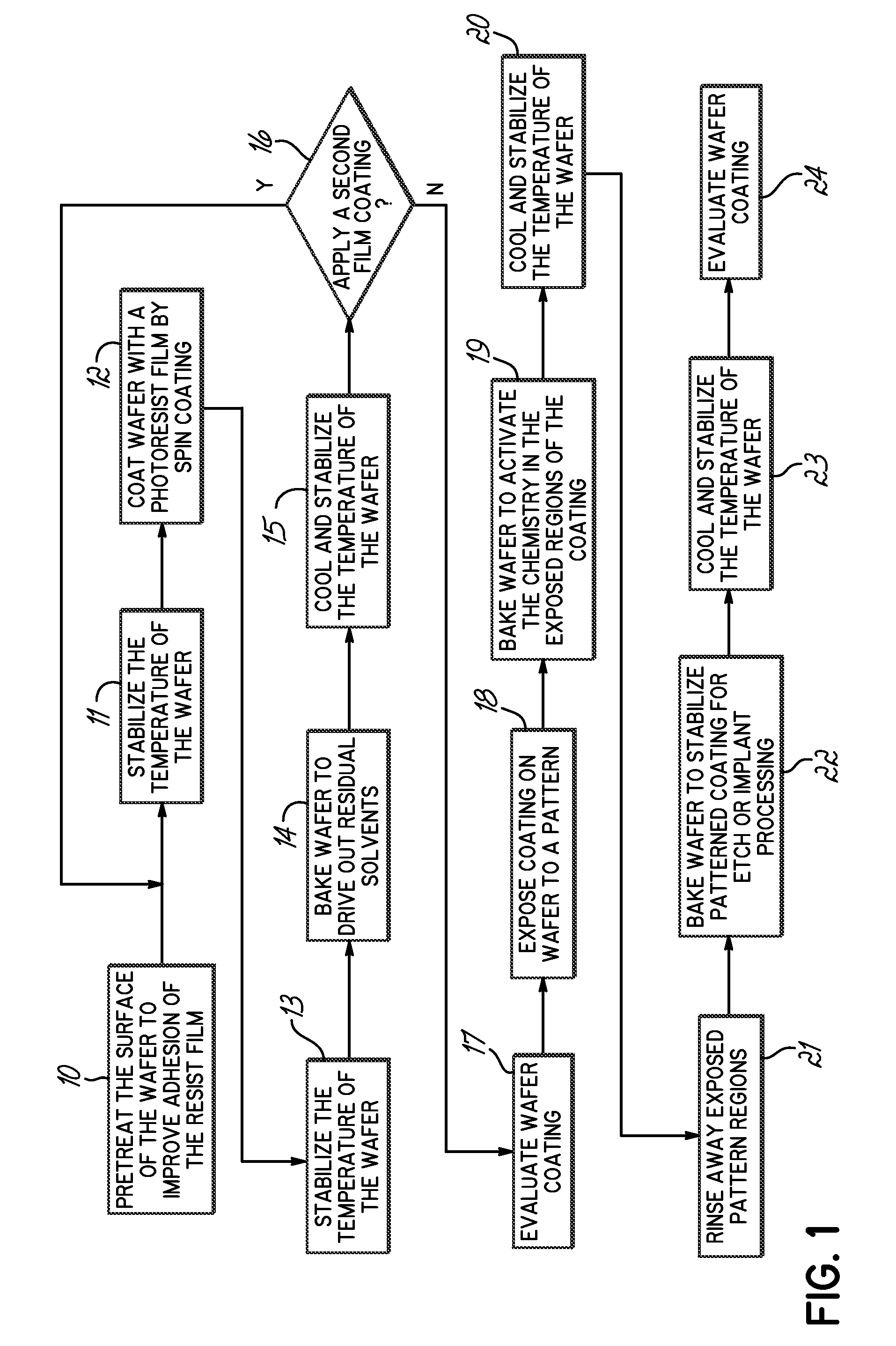
[0027]Photolithography processes for manufacturing semiconductor devices are divided into a series of lithography sequences. Each sequence may add a layer on to what may eventually become a multi-layer device. There are many different options that may be contained in any particular sequence. FIG. 1 shows an exemplary lithography sequence that may be used in conjunction with the present invention.

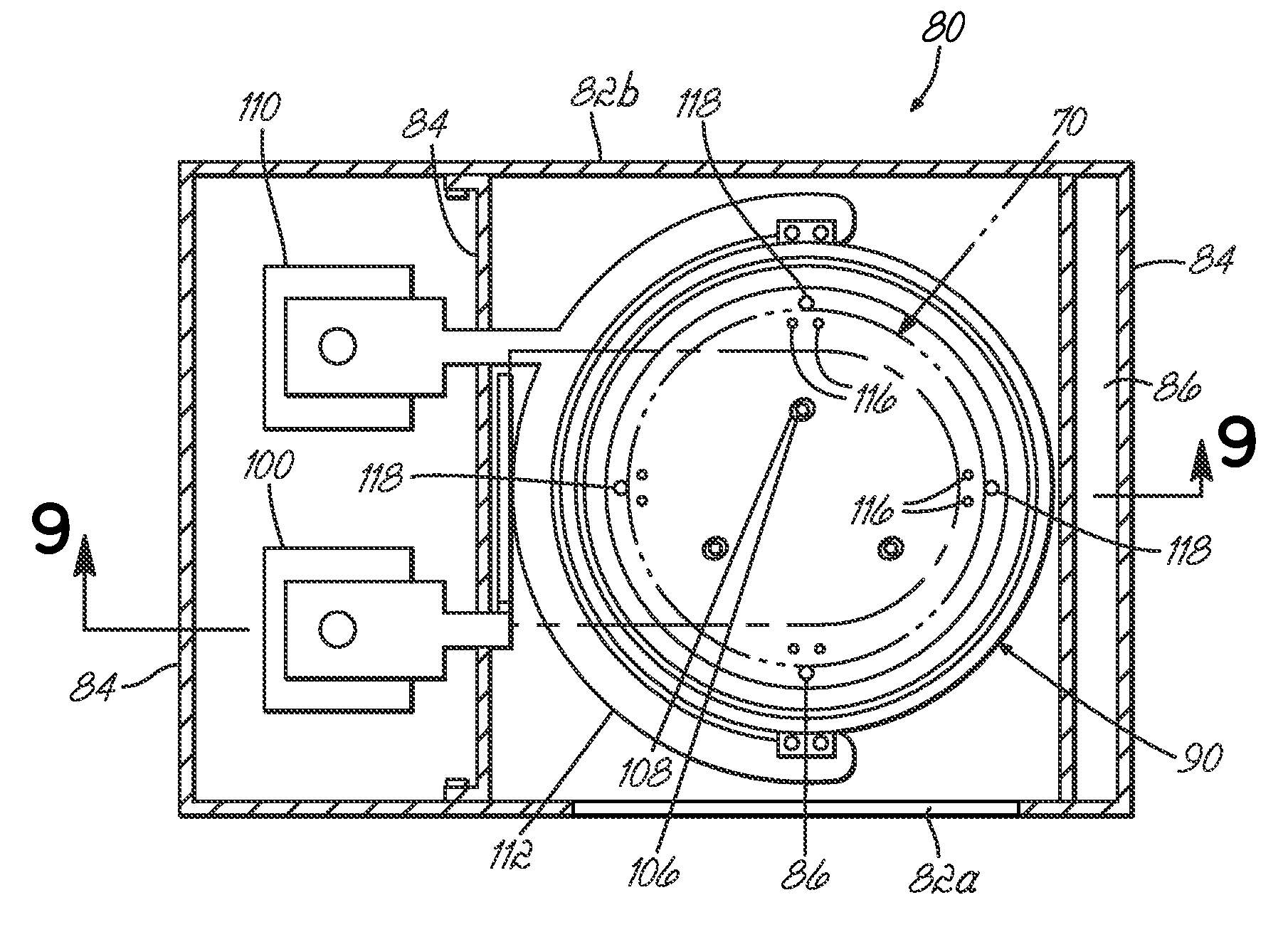
[0028]Referring now to FIG. 1, a wafer is loaded on to a coating / developing unit, also known as a Track tool, for processing. In block 10, the wafer may first be transferred to a vapor prime module on the Track tool where the wafer receives a pre-treatment to a surface to improve adhesion of a photoresist coating that will be applied to the wafer. In block 11, the wafer may then be transferred to a cool plate to stabilize the wafer temperature prior to coating. In block 12, once stabilized, the wafer may be transferred to a spin coating device where the wafer is coated by spinning the wafer ...


PUM


Abstract

A thermal processing apparatus and method with predictive temperature correction. Distances are measured from a backside of the wafer relative to a reference plane. Heat is transferred to the backside of the substrate in relation to the measured distances. This allows a baking unit to uniformly heat the substrate to compensate for irregularities or warpage.

Description

FIELD OF THE INVENTION[0001]The invention relates to an apparatus and methods for thermally processing substrates, such as semiconductor wafers.BACKGROUND OF THE INVENTION[0002]Coating / developing units, using photolithography processes for manufacturing semiconductor devices and liquid crystal displays (LCD's), generally coat a resist on a substrate, expose the resist coating to light to impart a latent image pattern, and develop the exposed resist coating to transform the latent image pattern into a final image pattern having masked and unmasked areas. This permits deposition or treatment of selected portions of the surface of the semiconductor wafer. Such a series of processing stages is typically carried out in a coating / developing system having discrete heating sections, such as a post apply baking unit and a post exposure baking unit. Each heating section of the coating / developing system incorporates a hotplate with a built-in heater.[0003]Feature sizes of semiconductor device ...

Claims


Application Information

Patent Timeline
IPC IPC(8): F27D13/00
CPCF27B17/0025H01L21/67109H01L21/67248H01L21/67259
Inventor KULP, JOHN
Owner TOKYO ELECTRON LTD
Why Eureka
Try Eureka