Inline physical shape profiling for predictive temperature correction during baking of wafers in a semiconductor photolithography process

Inactive Publication Date: 2008-09-16
TOKYO ELECTRON LTD
View PDF11 Cites 14 Cited by
  • Summary
  • Abstract
  • Description
  • Claims
  • Application Information

AI Technical Summary

Benefits of technology

[0008]Since the ramp up of the temperature of a cold wafer is a dynamic event, small adjustments in control set points will stabilize during the ramp event. By this method, each wafer will see a customized heating event matching the physical shape of that individual wafer.

Problems solved by technology

However, there is an uncontrolled phenomena in the production implementation of this PEB process that is likely to cause severe issues as feature sizes continue to decrease.
The phenomena, or problem, is that the hot plates are precisely calibrated using a flat bare silicon wafer with imbedded thermal sensors.
But actual production wafers with deposited films on the surface of the silicon exhibit small amounts of warpage due to the stresses induced by the deposited film

Method used


Image

  • Inline physical shape profiling for predictive temperature correction during baking of wafers in a semiconductor photolithography process
  • Inline physical shape profiling for predictive temperature correction during baking of wafers in a semiconductor photolithography process
  • Inline physical shape profiling for predictive temperature correction during baking of wafers in a semiconductor photolithography process

Examples


Example

[0018]According to the present invention, a semi-conductor wafer is heated on a hot plate during the processing steps and generally subsequent to application of a chemically amplified resist.

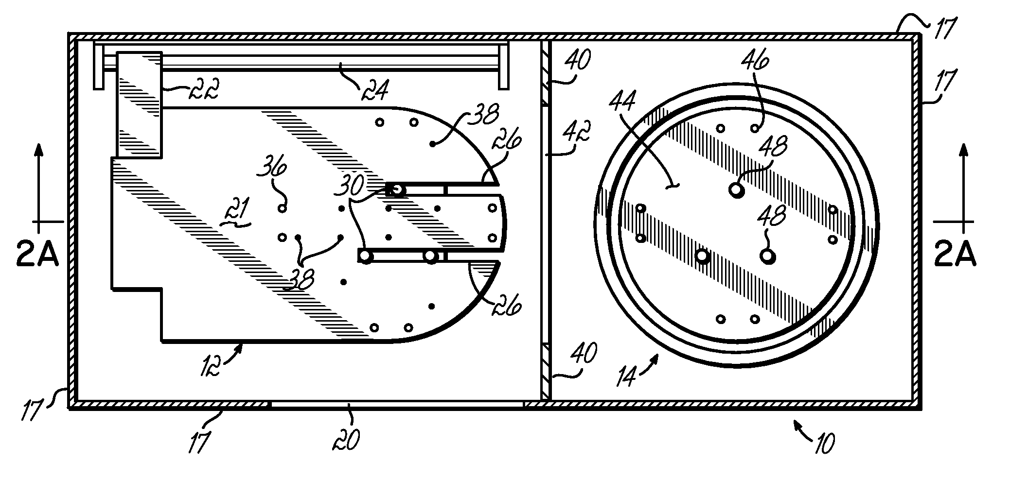
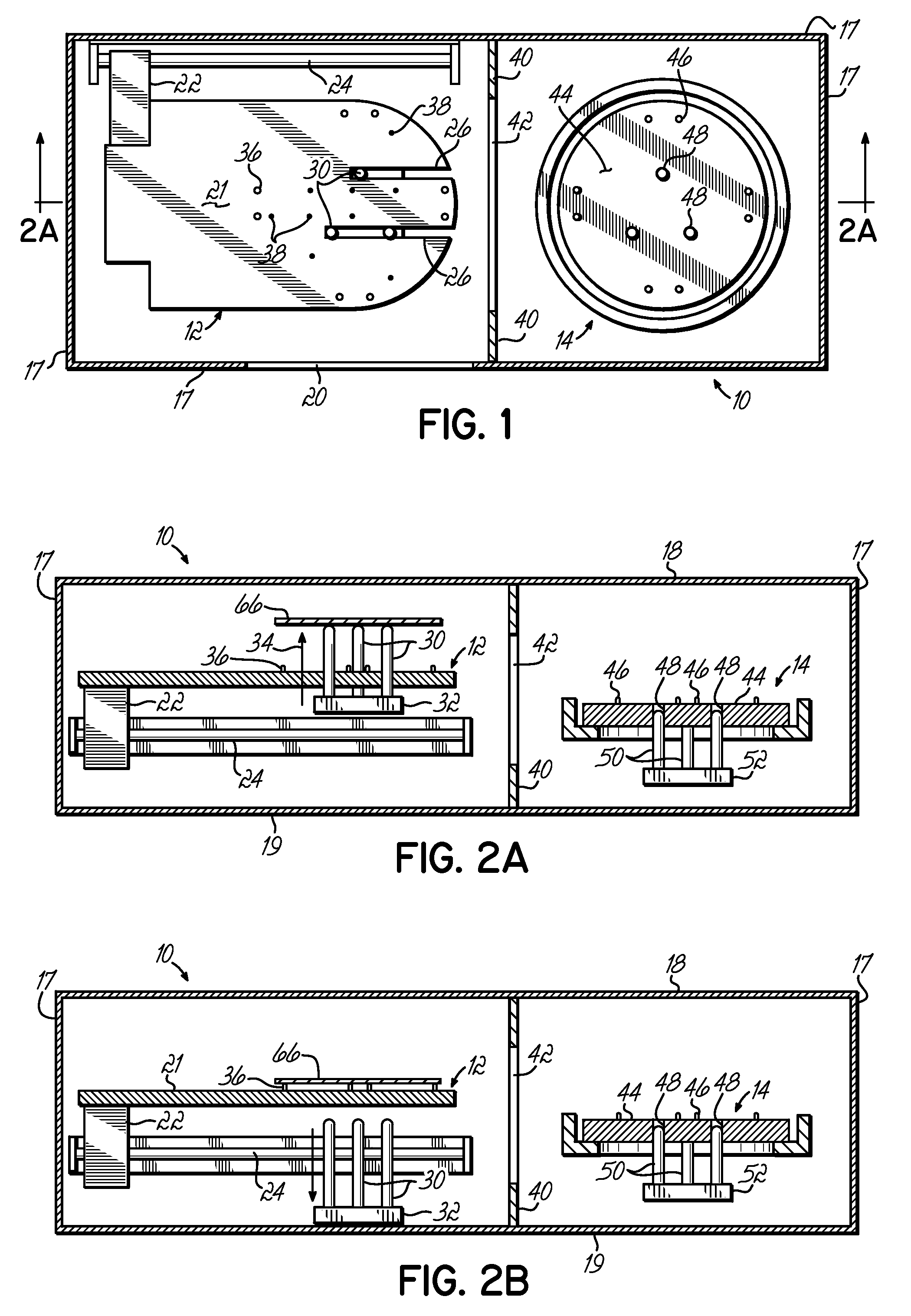
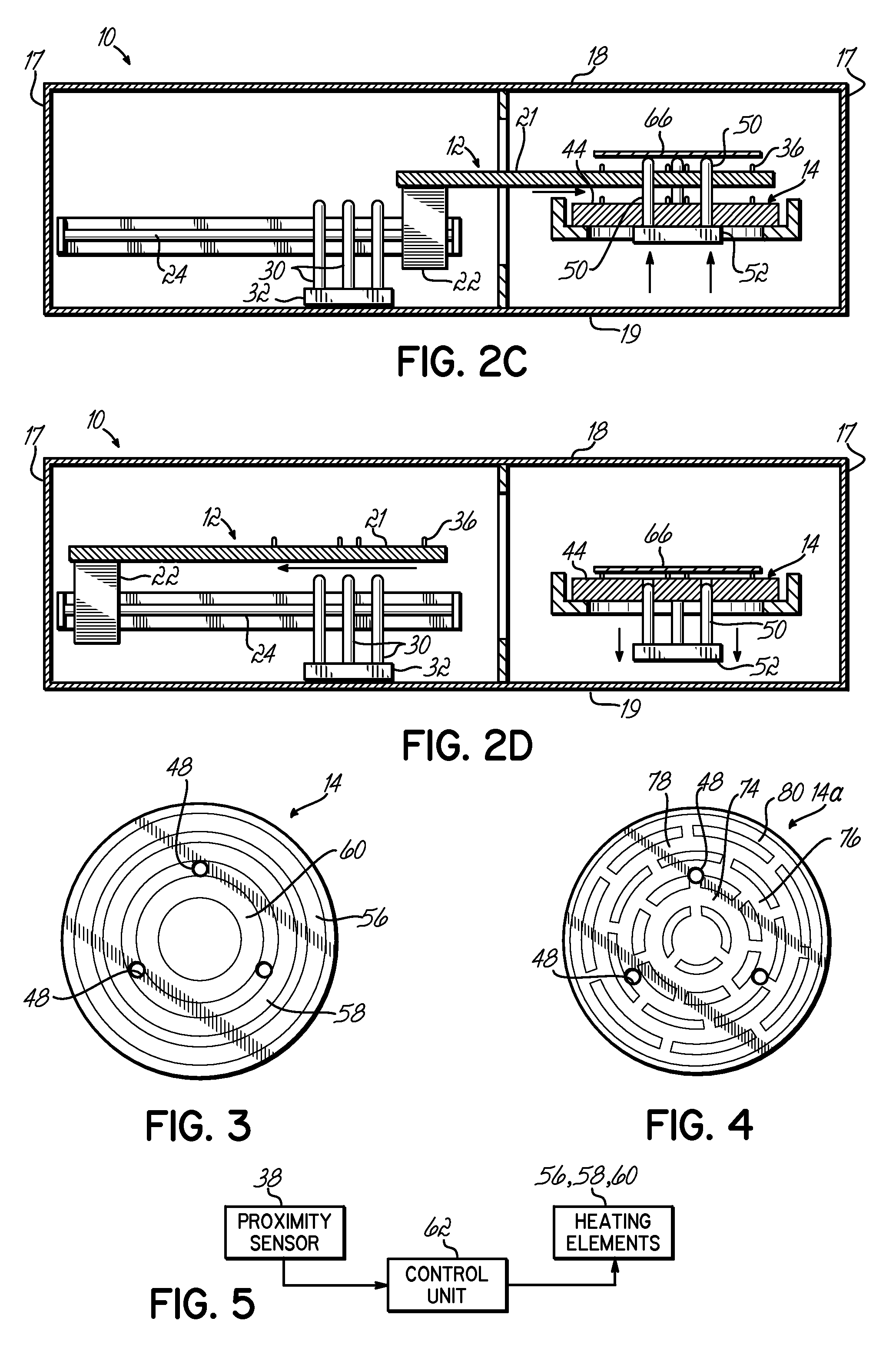
[0019]The topography of the bottom surface of the semiconductor wafer is measured during processing immediately prior to locating the semiconductor wafer on a hot plate. A plurality of distances from a common plane to the bottom surface of the semiconductor wafer are measured. That information is then transferred to a control unit for the heating plate. The hot plate in turn is controlled to establish a plurality of heating zones corresponding to the measured locations and selectively heat areas of the semi-conductor wafer on the heating plate to compensate for differences in measured distances.

[0020]An apparatus or module 10 for practicing the present invention includes a cool plate 12 and a hot plate 14. The module 10 is surrounded by an exterior casing 16 which includes sidewalls 17 and top a...


PUM

PropertyMeasurementUnit
Temperatureaaaaaaaaaa
Distanceaaaaaaaaaa

Abstract

The post exposure bake cycle in a chemically amplified resist process is more precisely controlled by measuring the distance from multiple locations on the bottom of each processed wafer to a reference plane surface while the wafer is supported on a cool plate. Subsequent to measuring the distance, the wafers are transferred to the hot plate that has a series of controllable heating elements. The set temperature for the heating elements is established in response to the distances measured while the wafer is on the cooling plate. The measurements are taken by utilizing proximity sensors located within the cooling plate.

Description

FIELD OF THE INVENTION[0001]This invention relates to a method and apparatus to subject a semiconductor wafer to a post exposure bake (PEB).BACKGROUND OF THE INVENTION[0002]In the semiconductor photolithography process, the bake cycles are extremely important for uniformity and repeatability of the various process steps, with the most significant being the post exposure bake (PEB) cycle in a chemically amplified resist process. In this process, a photoresist is applied to the semiconductor surface. The photoresist is subjected to a mask exposure to apply a circuit pattern. Chemically amplified resists require both an exposure dose to generate a latent acid image, and a thermal dose to drive the deblocking reaction that changes the solubility of the resist. The post exposure bake must optimize the balance between relative rates of the diffusion and reaction processes.[0003]Hot plates having uniformities within a range of a few tenths of a degree centigrade are currently available and...

Claims


Application Information

Patent Timeline
IPC IPC(8): H05B3/68C23C16/00
CPCH01L21/67109H01L21/67748H01L21/67248
Inventor KULP, JOHN M.
Owner TOKYO ELECTRON LTD
Why Eureka
Try Eureka