Thin film transistor array panel and fabricating method thereof, and flat panel display with the same

a thin film transistor and array panel technology, applied in thermoelectric devices, instruments, optics, etc., can solve the problems of pixel defects, and deterioration of organic thin film transistor characteristics, so as to improve the characteristics of organic thin film transistor and the aperture ratio of the flat panel display

Inactive Publication Date: 2008-10-23
SAMSUNG ELECTRONICS CO LTD
View PDF6 Cites 22 Cited by
  • Summary
  • Abstract
  • Description
  • Claims
  • Application Information

AI Technical Summary

Benefits of technology

[0020]Systems and methods are disclosed, in accordance with one or more embodiments, to provide an organic thin film transistor array panel and a flat panel display

Problems solved by technology

On the other hand, if a bank having a small area is formed for improving the aperture ratio of the display device, the organic semiconductor material may overflow during the solution process such as inkjet printing such that the characteristics of the organic thin film transistors may be deteriorated and pixel defects may occur.
If the organic thin film transistor is used for the electrophoretic display and electrophoretic particles are

Method used


Image

  • Thin film transistor array panel and fabricating method thereof, and flat panel display with the same
  • Thin film transistor array panel and fabricating method thereof, and flat panel display with the same
  • Thin film transistor array panel and fabricating method thereof, and flat panel display with the same

Examples


exemplary embodiment 1

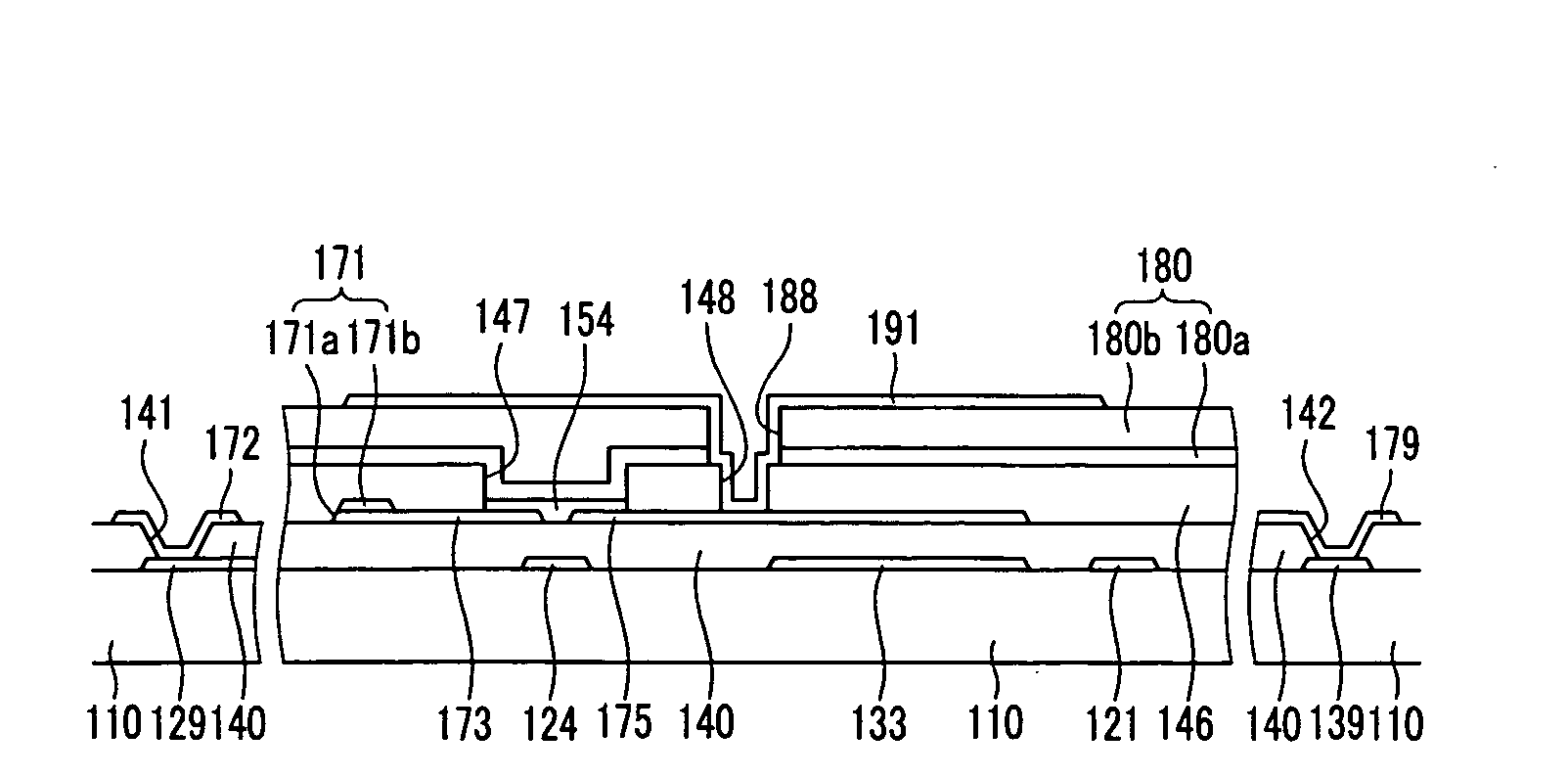
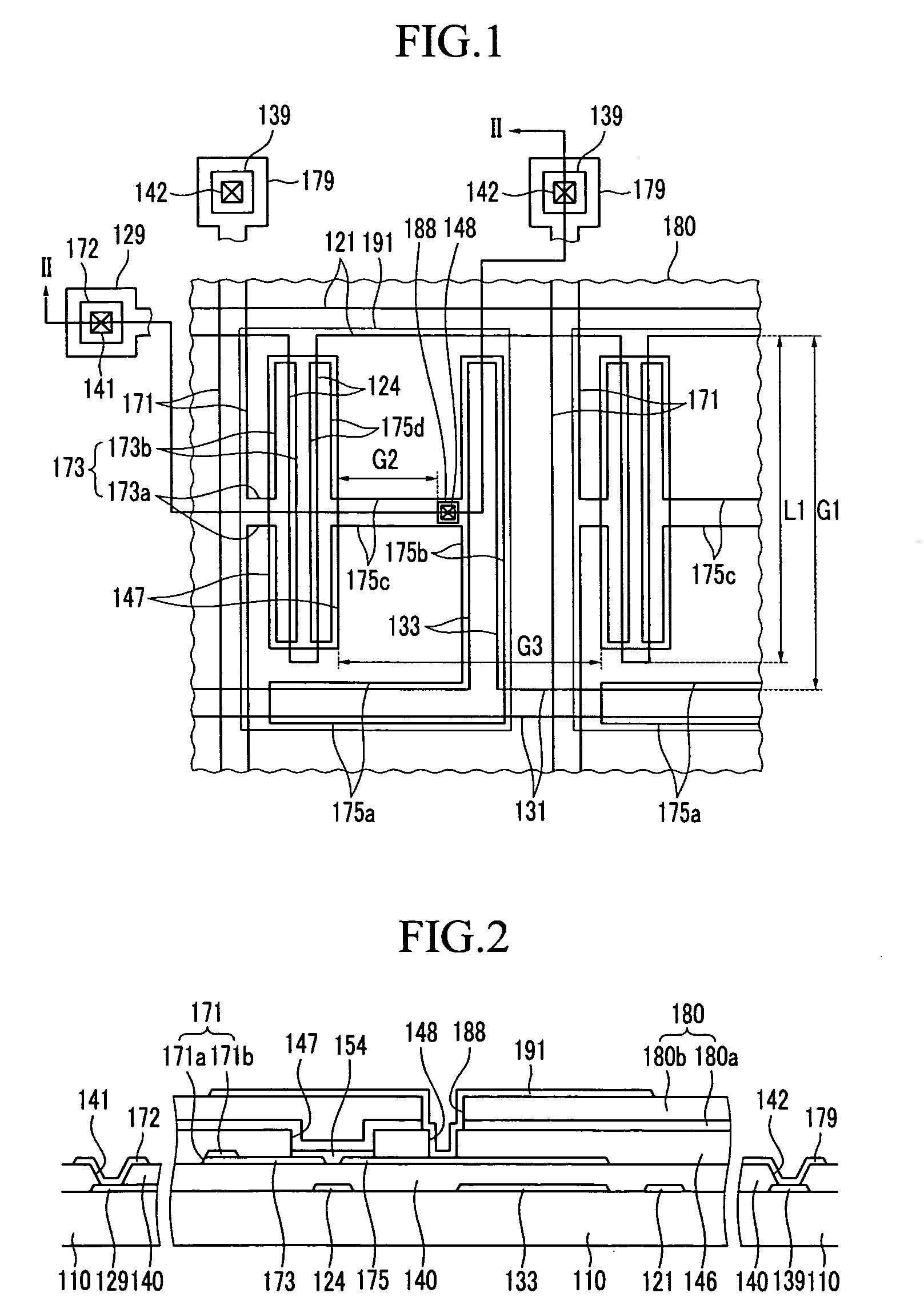
[0087]An organic thin film transistor array panel according to an embodiment of the present invention will be described in detail with reference to FIG. 1 and FIG. 2.

[0088]FIG. 1 is a layout view of an organic thin film transistor array panel according to an embodiment of the present invention, and FIG. 2 is a sectional view of the organic thin film transistor array panel shown in FIG. 1 taken along the line II-II.

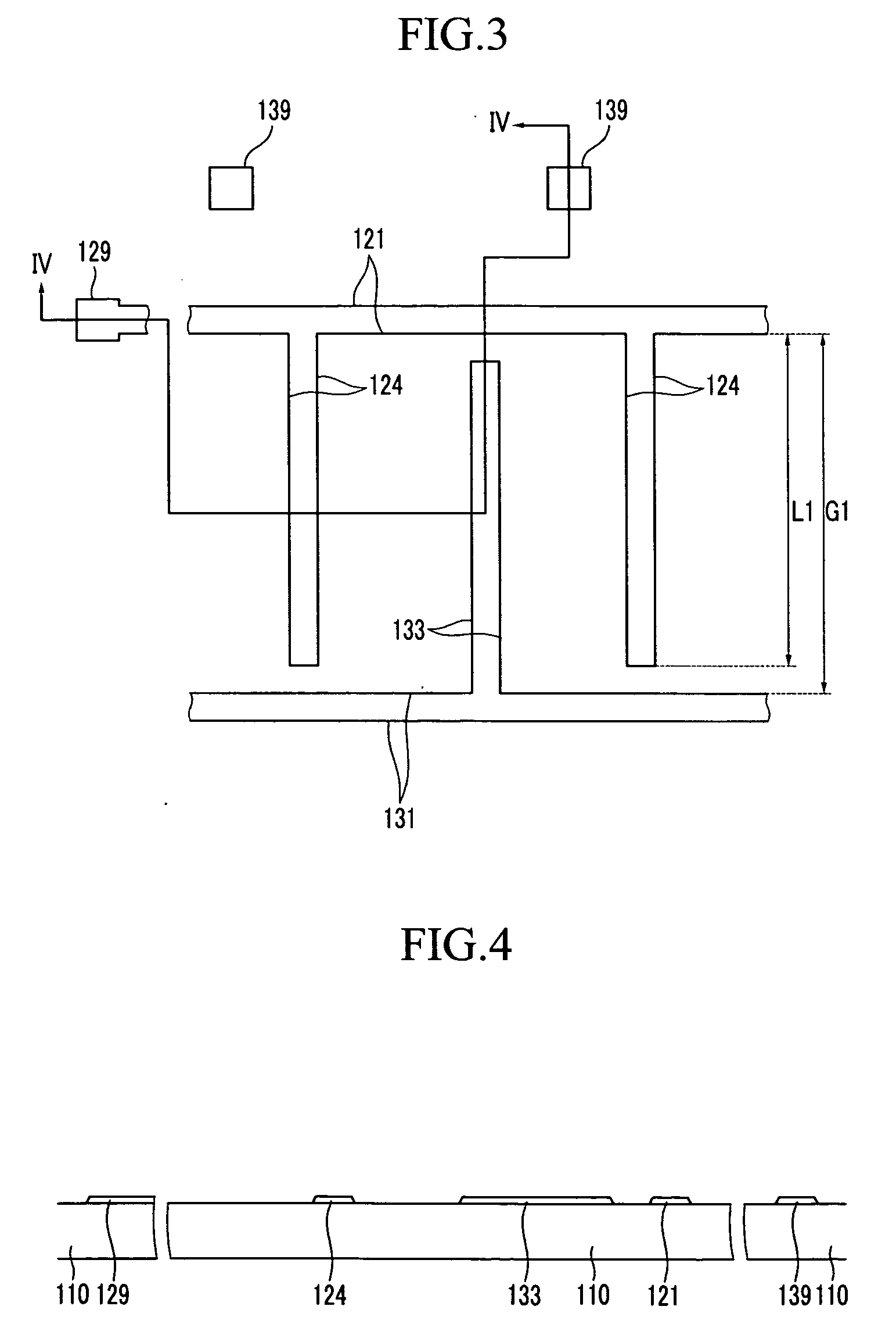
[0089]A plurality of gate lines 121, a plurality of storage electrode lines 131, and a plurality of data pads 139 are formed on an insulating substrate 110 made of a material such as transparent glass, silicone, or plastic.

[0090]The gate lines 121 transmit gate signals and extend substantially in a first direction (a transverse direction shown in FIG. 1). Each gate line 121 includes a plurality of gate electrodes 124 projecting in a second direction (a longitudinal direction shown in FIG. 1).

[0091]Each gate line 121 includes an end portion 129 having a large area for conta...

exemplary embodiment 2

[0161]An organic thin film transistor array panel according to another embodiment of the present invention will be described in detail with reference to FIG. 1 and FIG. 11. FIG. 11 is a sectional view of the organic thin film transistor array panel according to another embodiment of the present invention taken along the line II-II shown in FIG. 1.

[0162]As shown in FIG. 1 and FIG. 11, a layered structure of an organic thin film transistor array panel according to the present embodiment is substantially the same as that shown in FIG. 1 and FIG. 2.

[0163]A plurality of gate lines 121, a plurality of storage electrode lines 131, and a plurality of data pads 139 are formed on an insulating substrate 110. Each gate line 121 includes a plurality of gate electrodes 124 and an end portion 129 having a large area, each of the storage electrode lines 131 includes a plurality of storage electrodes 133 extending toward the gate line 121, and the data pads 139 are connected to end portions 179 of ...

exemplary embodiment 3

[0184]Now, a flat panel display including a thin film transistor array panel according to an embodiment of the present invention will be described in detail with reference to FIG. 18. FIG. 18 is a sectional view of an electrophoretic display including the organic thin film transistor array panel shown in FIG. 1 and FIG. 2. Even though an electrophoretic display is shown in FIG. 18, the thin film transistor array panel according to an embodiment of the present invention may be applied to other flat panel displays such as a liquid crystal display, an organic light emitting device, etc.

[0185]The electrophoretic display includes the thin film transistor array panel shown in FIG. 1 and FIG. 2. Accordingly, descriptions of constituent elements of the organic thin film transistor array panel may be omitted. Many characteristics of the organic thin film transistor array panel shown in FIG. 1 and FIG. 2 can be applied to the electrophoretic display according to the present embodiment.

[0186]T...


PUM


Abstract

An organic thin film transistor array panel, for an embodiment, includes a plurality of pixel electrodes formed on a top layer to cover organic thin film transistors, with display areas defined by the areas of the pixel electrodes. Accordingly, the aperture ratio of the display device may be increased. A ratio of width to length (W/L) in a channel of an organic thin film transistor may be increased, and thereby on current (Ion) of the organic thin film transistor may be increased. The organic semiconductor may be prevented from overflowing while being formed in holes by an inkjet printing method such that deterioration of thin film transistor characteristics and pixel defects is prevented. The adhesive of the electrophoretic sheet is prevented from penetrating into the organic semiconductor when the electrophoretic display is formed by attaching the electrophoretic sheet to the organic thin film transistor array panel by a lamination method.

Description

CROSS-REFERENCE TO RELATED APPLICATION[0001]This application claims priority to and the benefit of Korean Patent Application Nos. 10-2007-0039415 and 10-2007-0088268 filed in the Korean Intellectual Property Office on Apr. 23, 2007 and Aug. 31, 2007, respectively, the entire contents of which are incorporated herein by reference.BACKGROUND[0002](a) Technical Field[0003]Embodiments of the present invention relate generally to an organic thin film transistor array panel and a flat panel display including the organic thin film transistor array panel.[0004](b) Description of the Related Art[0005]A thin display device that is driven with a low voltage and is substantially flat is referred to as a flat panel display. The flat panel display includes a liquid crystal display, an electrophoretic display, etc. The flat panel display includes a plurality of pairs of field generating electrodes and an electro-optical active layer interposed therebetween.[0006]One electrode of each pair of field...

Claims


Application Information

Patent Timeline
IPC IPC(8): H01L51/05H01L51/40H01L29/786H01L21/336G02F1/167
CPCG02F1/1368G02F1/167G02F2202/022H01L51/0005H01L51/0545H10K71/135H10K10/466
Inventor SONG, KEUN-KYUCHO, SEUNG-HWANNOH, JUNG-HUN
Owner SAMSUNG ELECTRONICS CO LTD
Why Eureka
Try Eureka