Semiconductor Device

a semiconductor device and semiconductor technology, applied in semiconductor devices, digital storage, instruments, etc., can solve the problems of power consumption of memory accounts, and achieve the effect of suppressing heat generation and reducing power consumption of semiconductor devices according to the present invention

Inactive Publication Date: 2008-10-23
SEMICON ENERGY LAB CO LTD
View PDF12 Cites 4 Cited by
  • Summary
  • Abstract
  • Description
  • Claims
  • Application Information

AI Technical Summary

Benefits of technology

[0007]The present invention is devised in view of the above problems. An object of the present invention is to reduce the power consumption of a semiconductor device including a memory and a circuit (e.g. CPU, dedicated circuit, and the like) operating with the use of data stored in the memory.
[0008]Another object of the present invention is to reduce the power consumption of a semiconductor device by determining configurations of memory cells according to data stored in a memory circuit (e.g. data used in the CPU or in the dedicated circuit) and to provide semiconductor device with less heat generation.
[0013]Power consumption of the semiconductor device according to the present invention can be reduced by forming a memory cell with no semiconductor element. Furthermore, heat generation can be suppressed owing to the low power consumption.

Problems solved by technology

As a result, power consumption of the memory accounts for the major part of that of a circuit portion.

Method used


Image

  • Semiconductor Device
  • Semiconductor Device
  • Semiconductor Device

Examples


embodiment mode 1

[0032]In Embodiment Mode 1, an explanation of a semiconductor device including a memory and a CPU will be given. FIG. 3 is a block diagram showing a configuration example of the semiconductor device including the memory and the CPU.

[0033]As is shown in FIG. 3, the semiconductor device includes a CPU 151, a main memory 152, an input / output interface 153, an address bus 156, a data bus 157, and a controller bus 158. The main memory 152 includes a ROM 154 and a RAM 155. The ROM 154 is used as a program memory which stores a program executed by the CPU 151. The RAM 155 serves as a working memory for executing a program by the CPU 151.

[0034]The CPU 151 and the main memory 152 are connected via the address bus 156. Furthermore, the CPU 151, the main memory 152, and the input / output interface 153 are connected to each other via the data bus 157 and the controller bus 158.

[0035]The CPU 151 controls operation of an apparatus, and data required for the CPU 151 to execute a program is stored i...

embodiment mode 2

[0078]As is described in Embodiment Mode 1, a memory circuit can be configured to minimize the power consumption by analyzing the data of a program required by the CPU in the CPU and the memory circuit storing a program (a program memory), which have a close relation with each other in a configuration of a semiconductor device.

[0079]In addition, even when the data of a program is not analyzed, the power consumption can be effectively reduced by changing the configuration of the memory according to data of NOP commands of the CPU. In Embodiment Mode 2, such an example will be described.

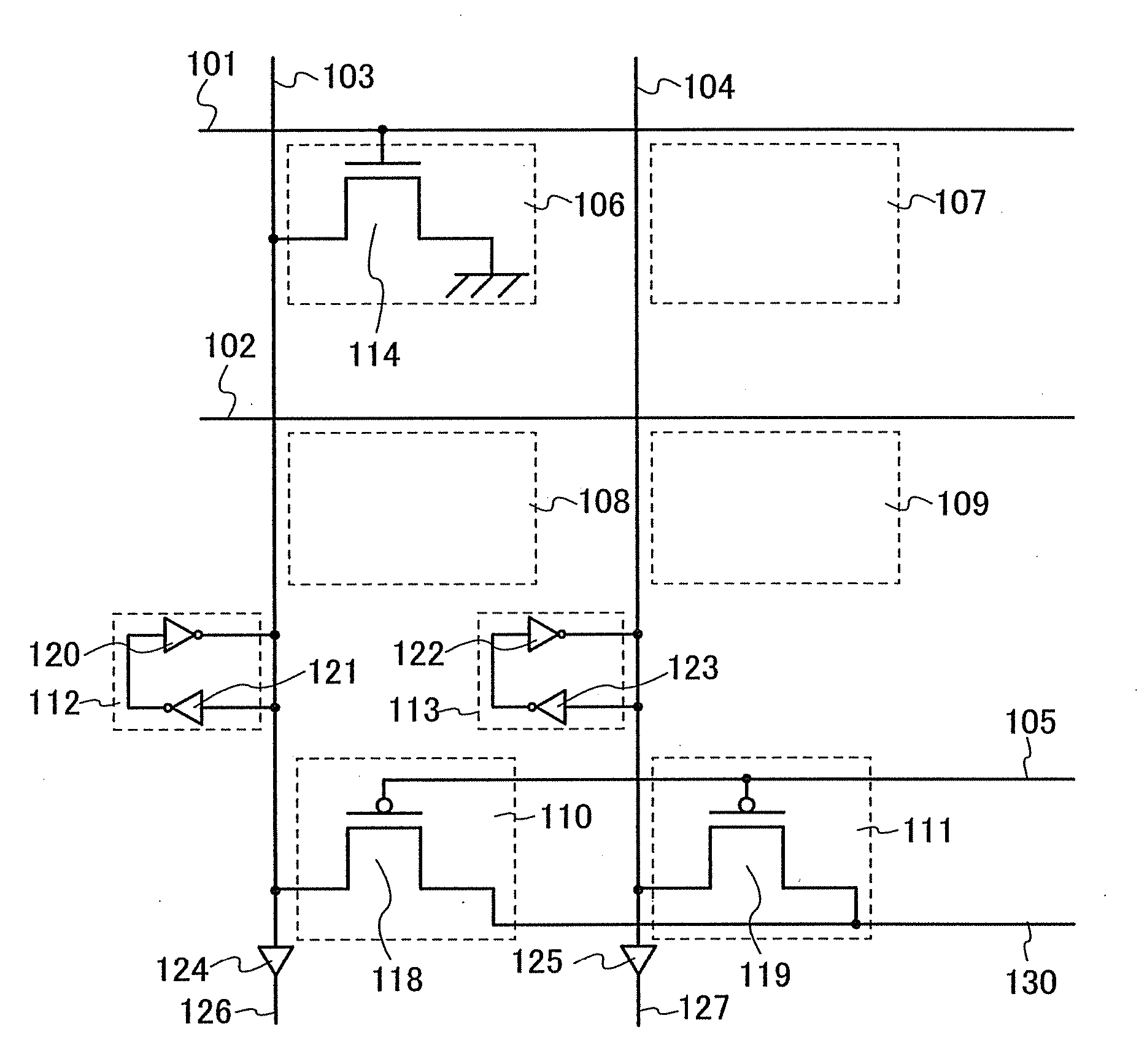
[0080]In Embodiment Mode 2, a plurality of memory cells storing a NOP command are composed of vacant cells in a memory circuit. For example, if a NOP command consists of “high” data (or “1”) only, the memory circuit as shown in FIG. 1 (the ROM 154) can be used for a program memory. In the configuration example shown in FIG. 1, the data of the NOP command is stored in the memory cells (108 and 109) whic...

embodiment mode 3

[0085]In Embodiment Mode 3, an example of a memory circuit provided with memory cells in place of vacant cells will be described. The memory cells have functions similar to the vacant cells. To be more specific, a semiconductor element, e.g. a transistor, is provided in a memory cell so that the memory cell can function in the similar way to a vacant cell, and the semiconductor element is not electrically connected to a word line. A memory cell including a semiconductor element which is not electrically connected to a word line as described above will be referred to as an “open cell”.

[0086]Hereinafter, a configuration example of a memory circuit according to Embodiment Mode 3 will be described with reference to FIG. 6. In Embodiment Mode 3, a configuration example is shown where “high” is a majority in the data stored in a memory circuit. The memory circuit shown in FIG. 6 has the same data array as that shown in FIG. 1, and the same reference numerals in FIGS. 1 and 6 indicate the ...


PUM


Abstract

A memory circuit includes a plurality of word lines, a plurality of bit lines, and a plurality of memory cells. Configurations of the plurality of memory cells are determined depending on the data (“high” or “low”) which is stored in the memory cells. Data array such as a program stored in the memory circuit is analyzed in advance. In the case where “high” is the majority data, memory cells storing “high” are formed with vacant cells in which a semiconductor element is not formed.

Description

BACKGROUND OF THE INVENTION[0001]1. Field of the Invention[0002]The present invention relates to a semiconductor device including a memory circuit.[0003]2. Description of the Related Art[0004]Now products with CPUs, e.g. appliances and computers, have spread in the world and serve as necessities in our life. Generally, these products are equipped with integrated circuit components such as a dedicated circuit having a specific function, a memory, and the like. For example, in a product with a CPU and a memory, the memory functions as a program storage area or working area of the CPU.[0005]As a product with a CPU and a memory, for example, a semiconductor device capable of radio communication as disclosed in Reference 1 (Hiroki Dembo et al, “RFCPUs on Glass and Plastic Substrates Fabricated by TFT Transfer Technology”, IEEE, TECHNICAL DIGEST OF INTERNATIONAL ELECTRON DEVICES MEETING, Dec. 5, 2005, pp. 1067-1069) is well known. Such a semiconductor device is called a wireless chip, wir...

Claims


Application Information

Patent Timeline
Patent Type & Authority Applications(United States)
IPC IPC(8): G11C7/00
CPCG11C7/12G11C16/0416G11C17/12H01L27/112H01L27/12H01L27/1214H10B20/00
Inventor KOZUMA, MUNEHIROKUROKAWA, YOSHIYUKI
Owner SEMICON ENERGY LAB CO LTD
Why Eureka
Try Eureka