Semiconductor Device and Semiconductor Integrated Circuit Device for Driving Plasma Display Using the Semiconductor Device

Inactive Publication Date: 2008-10-30
HITACHI LTD
View PDF1 Cites 18 Cited by
  • Summary
  • Abstract
  • Description
  • Claims
  • Application Information

AI Technical Summary

Benefits of technology

[0011]With a lateral IGBT according to an aspect of the present invention in which a silicon layer between a first conductivity-type, high concentration layer newly provided for covering emitter-gate regions and a buried oxide film is made to have a reduced resistance to increase current flowing to an emitter farther from a collector, whereby it

Problems solved by technology

However, with the IGBTs of the above-described conventional structure, those of the plural emitter-gate regions, provided between collector regions, which are farther from the collector regi

Method used


Image

  • Semiconductor Device and Semiconductor Integrated Circuit Device for Driving Plasma Display Using the Semiconductor Device
  • Semiconductor Device and Semiconductor Integrated Circuit Device for Driving Plasma Display Using the Semiconductor Device
  • Semiconductor Device and Semiconductor Integrated Circuit Device for Driving Plasma Display Using the Semiconductor Device

Examples


embodiment 1

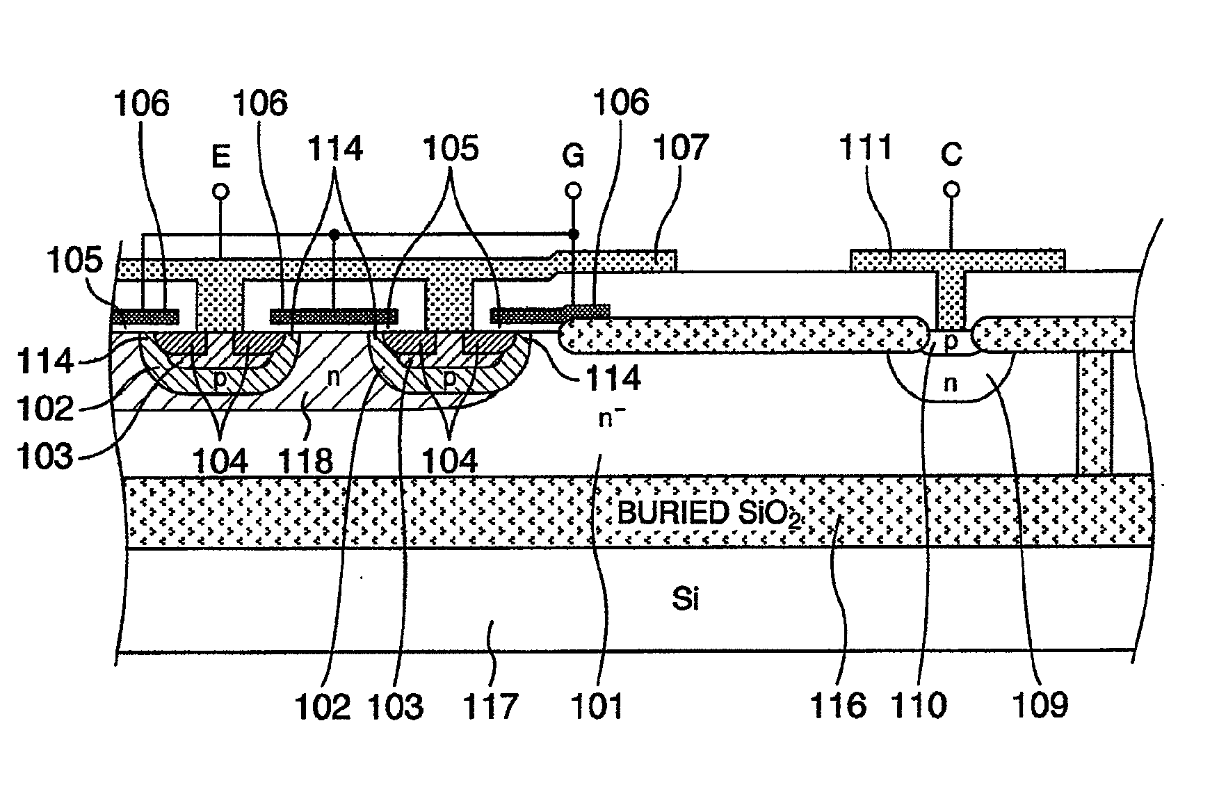
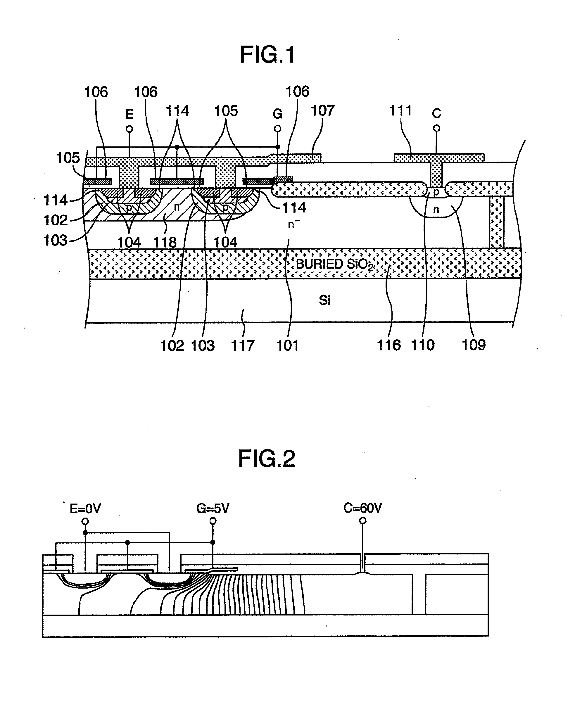
[0026]FIG. 1 is a sectional structural diagram showing a part of an IGBT according an embodiment of the present invention.

[0027]In FIG. 1, a buried oxide film 116 is formed on a Si support substrate 117 of an SOI substrate. Plural p-base regions 102 are formed selectively in a surface layer of an n-type semiconductor substrate 101. Two n-emitter regions 104 are formed in portions of a surface layer of each p-base region 102. A p-contact region 103 is formed, in each p-base region 102, between the two n-emitter regions 104 with its portions being overlapped with the two n-emitter regions 104. Plural n-buffer regions 109 are formed selectively in those of exposed surface portions of the n-type substrate 1 in which the p-base regions 102 are not formed. A p-collector region 110 is formed in a surface layer of each n-buffer region 109. Gate electrodes 106, which are connected with gate terminals (hereafter, referred to as “G-terminal”), are provided above a surface of a channel region 1...


PUM


Abstract

A lateral IGBT structure having an emitter terminal including two or more base layers of a second conductivity-type for one collector terminal, in which the base layers of a second conductivity-type in emitter regions are covered with a first conductivity-type layer having a concentration higher than that of a drift layer so that a silicon layer between the first conductivity-type layer covering the emitter regions and a buried oxide film has a reduced resistance to increase current flowing to an emitter farther from the collector to thereby enhance the current density.

Description

BACKGROUND OF THE INVENTION[0001]The present invention relates to lateral insulated-gate bipolar transistors (hereafter, referred to as “IGBT”) and semiconductor integrated circuits for driving a plasma display using such transistors.[0002]Recently, many high blocking voltage power ICs using an SOI substrate have been developed because of their features such that they only need small device isolation areas and are free from parasitic transistors. In developing high blocking voltage power ICs, it will be essential from the viewpoint of the output performances and chip size reduction that high blocking voltage power ICs which directly drive loads should have enhanced performances. However, in the lateral IGBTs, which are mainly employed as output devices in power ICs using an SOI substrate, emitter-gate regions and collector regions are formed on the same surface, which limits a substantial current conduction area to reduce the current capacity per device area.[0003]Furthermore, since...

Claims


Application Information

Patent Timeline
IPC IPC(8): H01L29/739G09G5/00G09G3/20G09G3/288G09G3/291G09G3/293G09G3/294G09G3/296G09G3/298H01L21/336H01L29/786
CPCG09G3/293G09G3/296G09G2330/04H01L29/7394
Inventor HARA, KENJISAKANO, JUNICHISHIRAKAWA, SHINJI
Owner HITACHI LTD
Why Eureka
Try Eureka