Method of Fabricating Semiconductor Device

a semiconductor and device technology, applied in the direction of semiconductor devices, basic electric elements, electrical appliances, etc., can solve the problems of increasing the stress within the channel junction, generating disturbances, and inevitable damage to the sidewall of the silicon (si) substrate by excessive si etching

Active Publication Date: 2008-10-30
SK HYNIX INC
View PDF27 Cites 12 Cited by
  • Summary
  • Abstract
  • Description
  • Claims
  • Application Information

AI Technical Summary

Benefits of technology

[0006]This invention is directed to a method of fabricating a semiconductor device wherein a P well is formed by performing an ion implantation process at a zero tilt condition, so that a stress caused by collision of a dopant and a Si lattice may be minimized. NOP fail due to disturbance caused by stress remaining within a channel junction of a semiconductor substrate may be reduced.

Problems solved by technology

Thus, etch damage to sidewall of a silicon (Si) substrate due to excessive Si etch is inevitable.
Stress within a channel junction may be increased by implant damage.
The increased stress grows into defects due to a subsequent annealing process, thus generating disturbances caused by Transit Enhanced Diffusion (TED).
In the case of a flash memory device on which program and erase may be performed using channel boosting, Number Of Program (NOP) fail occurs due to the existence of disturbances within the channel junction.
This becomes more severe at certain portions, which becomes a cause of remaining stress within an active region.
However, if the trenches are gap filled with the SOD material, dopant segregation may be increased due to the stress of the material and a subsequent annealing process.
Accordingly, the leakage current may be increased due to the occurrence of hump.
Furthermore, compensation for the lost dopant through additional ion implantation may cause cell disturbances to further increase.

Method used


Image

  • Method of Fabricating Semiconductor Device
  • Method of Fabricating Semiconductor Device
  • Method of Fabricating Semiconductor Device

Examples


Embodiment Construction

[0014]Now, specific embodiments according to the present invention will now be described in further details with reference to the accompanying drawings.

[0015]While the invention is susceptible to various manners, certain embodiments as shown by way of example in the drawings and these embodiments will be described in detail herein. It will be understood, however, that this disclosure is not intended to limit the invention to the particular forms described, but to the contrary, the invention is intended to cover all modifications, alternatives, and equivalents falling within the spirit and scope of the invention defined by the appended claims.

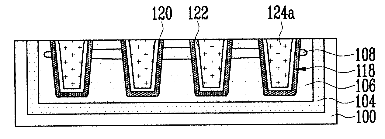
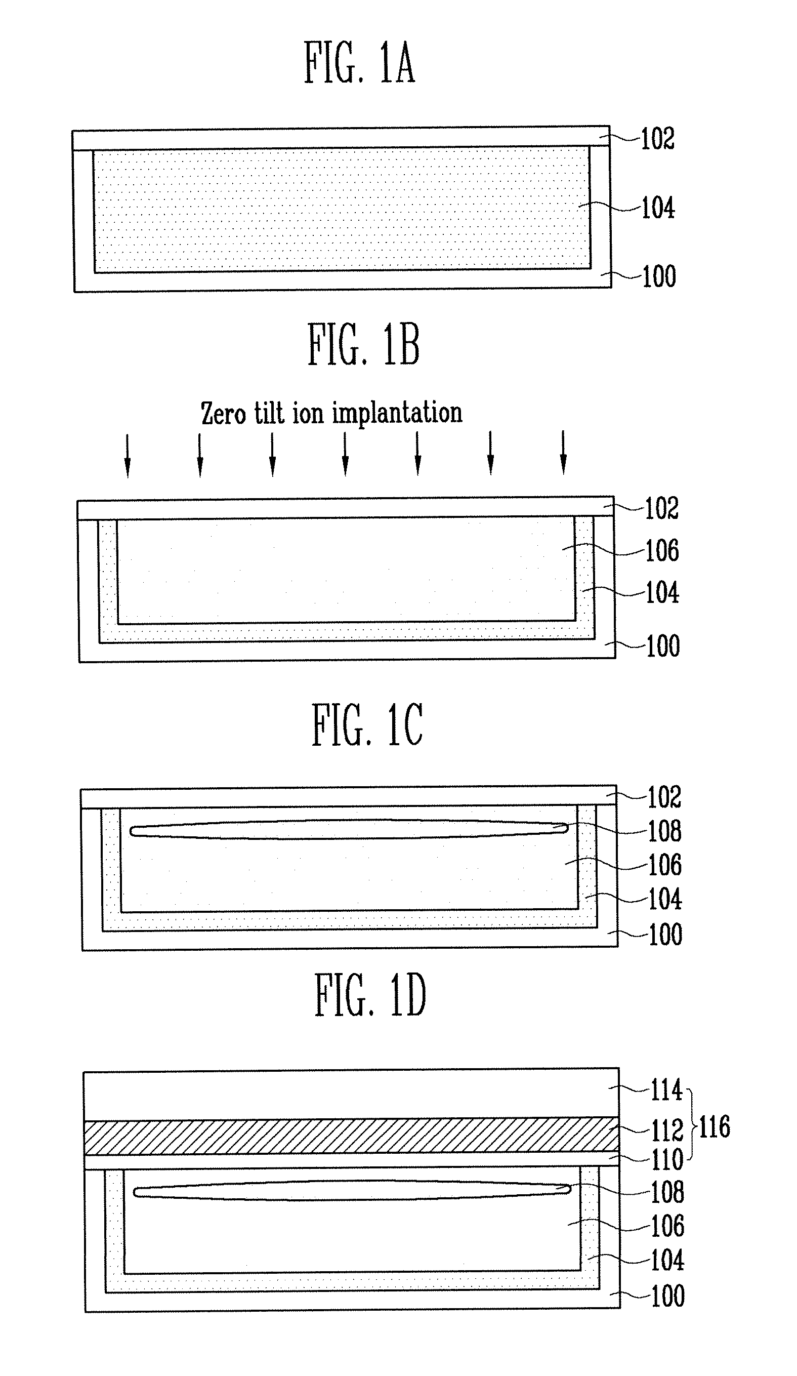
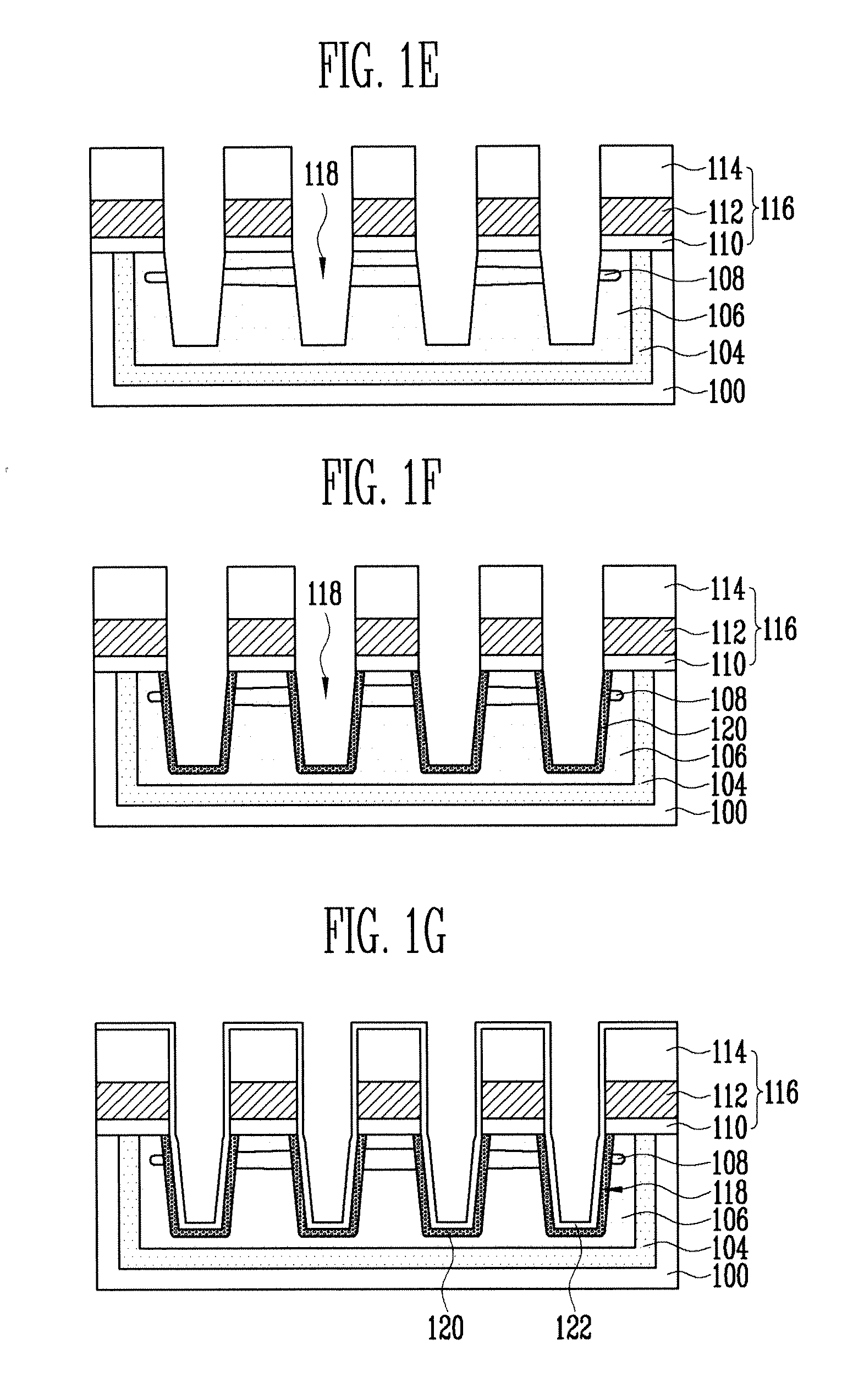
[0016]Referring to FIG. 1A, a screen oxide layer 102 is formed over a semiconductor substrate 100. The screen oxide layer 102 may be formed, for example, using an oxidation process, preferably, a wet oxidization process at a temperature ranging from 750 to 800 degrees Celsius. Other types of oxidation techniques may be used. The screen oxide lay...


PUM


Abstract

This invention relates to a method of fabricating a semiconductor device. A P well for a cell junction may be formed by performing an ion implantation process employing a zero tilt condition. Stress caused by collision between a dopant and a Si lattice within a semiconductor substrate may be minimized and, therefore stress remaining within the semiconductor substrate may be minimized. Accordingly, Number Of Program (NOP) fail by disturbance caused by stress remaining within a channel junction may be reduced. Further, a broad doping profile may be formed at the interface of trenches by using BF2 as the dopant when the P well is formed. A fluorine getter layer may be formed on an oxide film of the trench sidewalls and may be used as a boron diffusion barrier. Although a Spin On Dielectric (SOD) insulating layer may be used as an isolation layer, loss of boron (B) may be prevented. Accordingly, an additional ion implantation process for compensating for lost boron (B) may be omitted and a NOP disturbance characteristic may be improved.

Description

CROSS-REFERENCES TO RELATED APPLICATIONS[0001]This invention claims priority to Korean patent application number 10-2007-41414, filed on Apr. 27, 2007, the disclosure of which is incorporated by reference in its entirety.TECHNICAL FIELD[0002]This invention relates to a method of fabricating a semiconductor device and, more particularly, to a method of fabricating a semiconductor device with improved disturbance characteristic.BACKGROUND OF THE INVENTION[0003]Generally, in a semiconductor device, a well junction may be formed by performing an ion implantation process in order to control the threshold voltage of a transistor. In recent years, as devices are highly integrated, the well junction may be formed by implanting an impurity of a high concentration so as to secure the characteristics of the transistor when the ion implantation process is performed. Further, in forming a Shallow Trench Isolation (STI) layer a STI structure in which trenches may be formed in a semiconductor subs...

Claims


Application Information

Patent Timeline
Patent Type & Authority Applications(United States)
IPC IPC(8): H01L21/425
CPCH01L21/26506H01L21/26513H01L21/823878H01L21/823892H01L27/0928H01L21/2658H01L21/76
Inventor KWAK, NOH YEALJANG, MIN SIK
Owner SK HYNIX INC
Why Eureka
Try Eureka