Micro-protruding structure
a micro-protruding structure and micro-protruding technology, applied in the direction of separation processes, instruments, filtration separation, etc., can solve the problems of poor angular precision, poor positional precision, and inability to fully satisfy the characteristics of the micro-protruding structure required by the above fabrication method, so as to improve resolution, high positional precision, and improve the effect of resolution
- Summary
- Abstract
- Description
- Claims
- Application Information
AI Technical Summary
Benefits of technology
Problems solved by technology
Method used
Image
Examples
embodiment 1
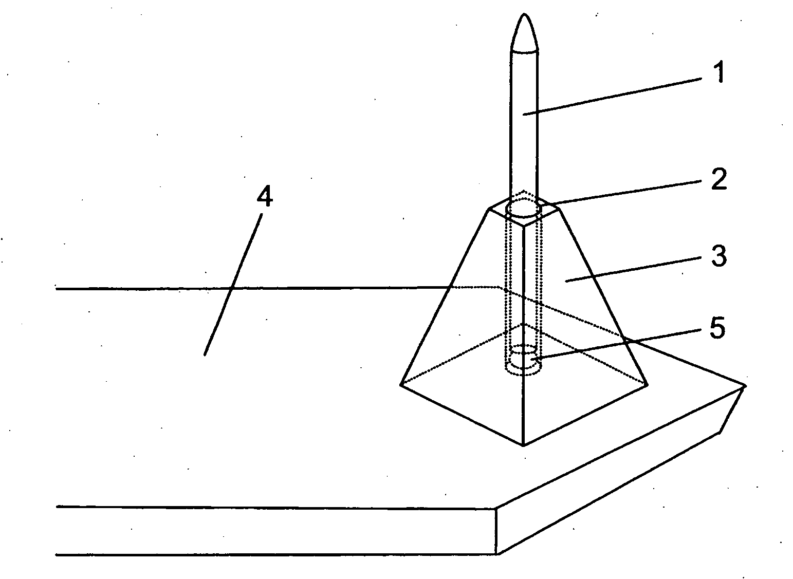
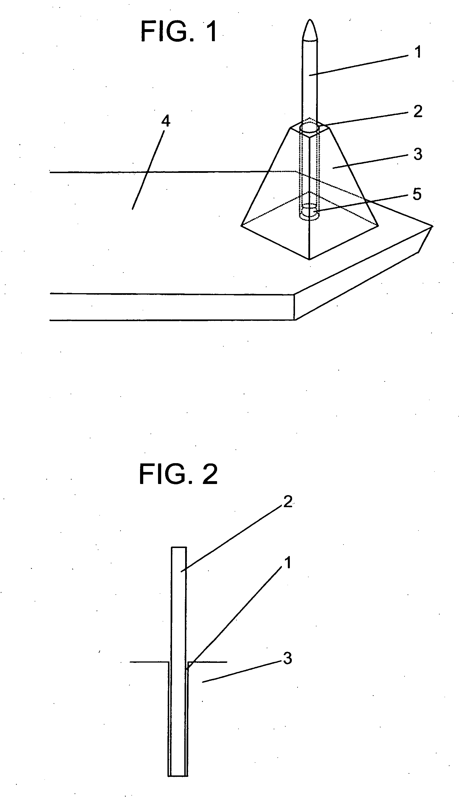
[0034]FIG. 1 is a view schematically illustrating the constitution of a micro-protruding structure according to a first embodiment of the invention provided on a cantilever of a scanning probe microscope. In FIG. 1, reference numeral 4 denotes a cantilever (cantilevered beam-type leaf spring) of a scanning probe microscope. At an end of the cantilever 4, there is formed a mother member 3 of a probe portion of the shape of a square truncated cone having a bottom side of about 10 μm. A fine hole structure 1 of a diameter of several tens of nanometers is formed in the central portion of the mother member 3 of the probe portion reaching from the upper surface to the bottom surface thereof nearly at right angles with the surface of the mother member 3 of the probe portion of the cantilever 4. A fine linear material 2 having an aspect ratio of not smaller than 10 is provided in the hole structure 1 so as to protrude outward from the bottom surface of the hole structure 1. The angular dire...
embodiment 2
[0038]FIG. 2 is a view schematically illustrating the micro-protruding structure according to a second embodiment of the invention. As an electron-emitting electrode, a linear material 2 of carbon nano-tube is inserted in the hole structure 1 provided vertically to the mother member 3 of the substrate. The hole structure 1 can be formed to in alignment with the center axis of the electron lens. The emission of electrons is homogeneously affected by an electric field, and the aberration of the electron beam is suppressed.
embodiment 3
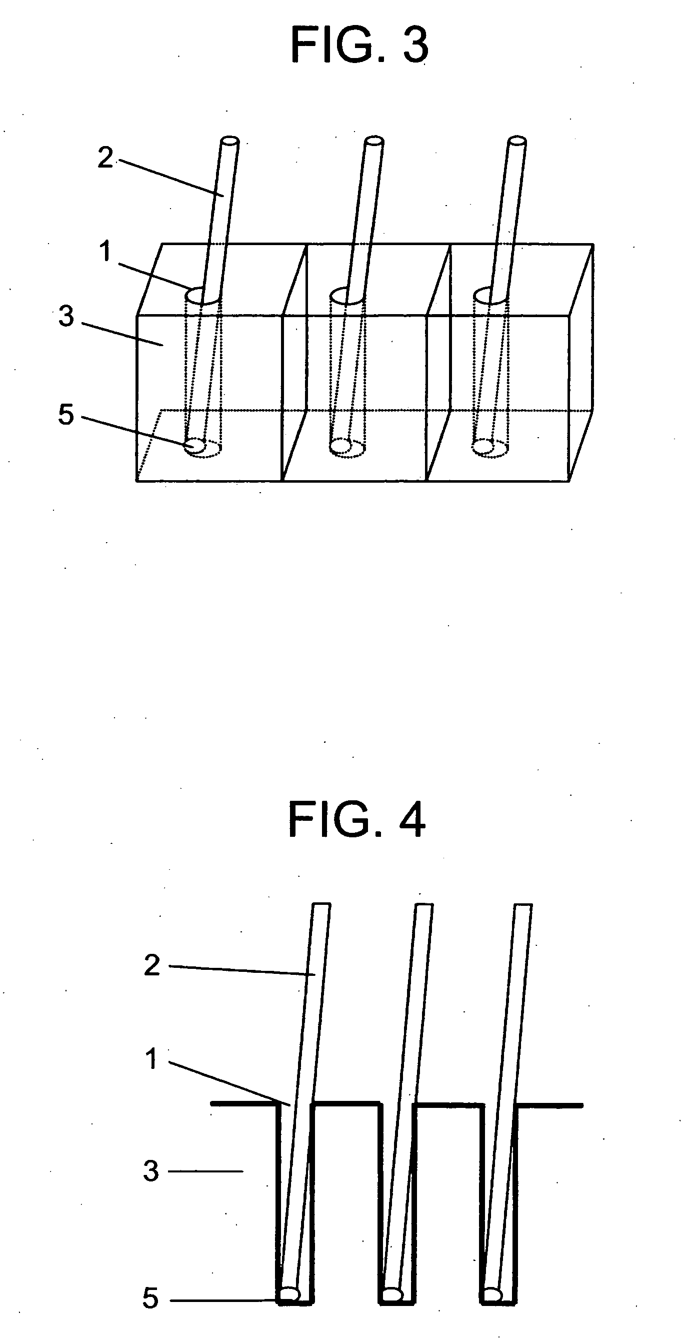
[0039]FIG. 3 is a view schematically illustrating the micro-protruding structure according to a third embodiment of the invention. FIG. 4 is a sectional view of the micro-protruding structure illustrated in FIG. 3. As electron-emitting electrodes, there are formed a plurality of micro-protruding structures to emit large amounts of electrons so as to be applied to a display element. By adjusting the density of the hole structures 1, the density of emitting electrodes can be controlled. The direction of the linear materials 2 is determined depending upon the angle of the hole structures, and can be constituted to be perpendicular to the electric field to draw out the electron-emitting efficiency to a maximum degree. The catalysts 5 are provided on the bottom surfaces of the hole structures 1, and the linear materials are grown to provide the structure at one time utilizing many hole structures.
PUM
| Property | Measurement | Unit |
|---|---|---|
| aspect ratio | aaaaa | aaaaa |
| diameter | aaaaa | aaaaa |
| length | aaaaa | aaaaa |
Abstract
Description
Claims
Application Information


