Semiconductor package substrate structure and manufacturing method thereof

Active Publication Date: 2008-11-06
UNIMICRON TECH CORP
View PDF4 Cites 7 Cited by
  • Summary
  • Abstract
  • Description
  • Claims
  • Application Information

AI Technical Summary

Benefits of technology

[0022]As for the semiconductor package substrate structure of the present invention and its manufacturing method, the electroplated conductive posts formed therein do not have wings like the prior art, thus stress caused by temperature variation is reduced. In addition, the electroplated conductive posts now fully encapsulate the tops and sides of the electrically connecting pads, a stronger bonding can be achieved. Moreover, since the width of the electrically connecting pads is similar to that of normal circuit layers, the width of the electroplated conductive posts can still be smaller than the conventional electroplated conductive posts with wings. Unlike the prior art where insulating protective layer is formed prior to the electroplating of the electroplated

Problems solved by technology

However, in the above prior-art manufacturing processes, the sizes of the openings

Method used


Image

  • Semiconductor package substrate structure and manufacturing method thereof
  • Semiconductor package substrate structure and manufacturing method thereof
  • Semiconductor package substrate structure and manufacturing method thereof

Examples


first embodiment

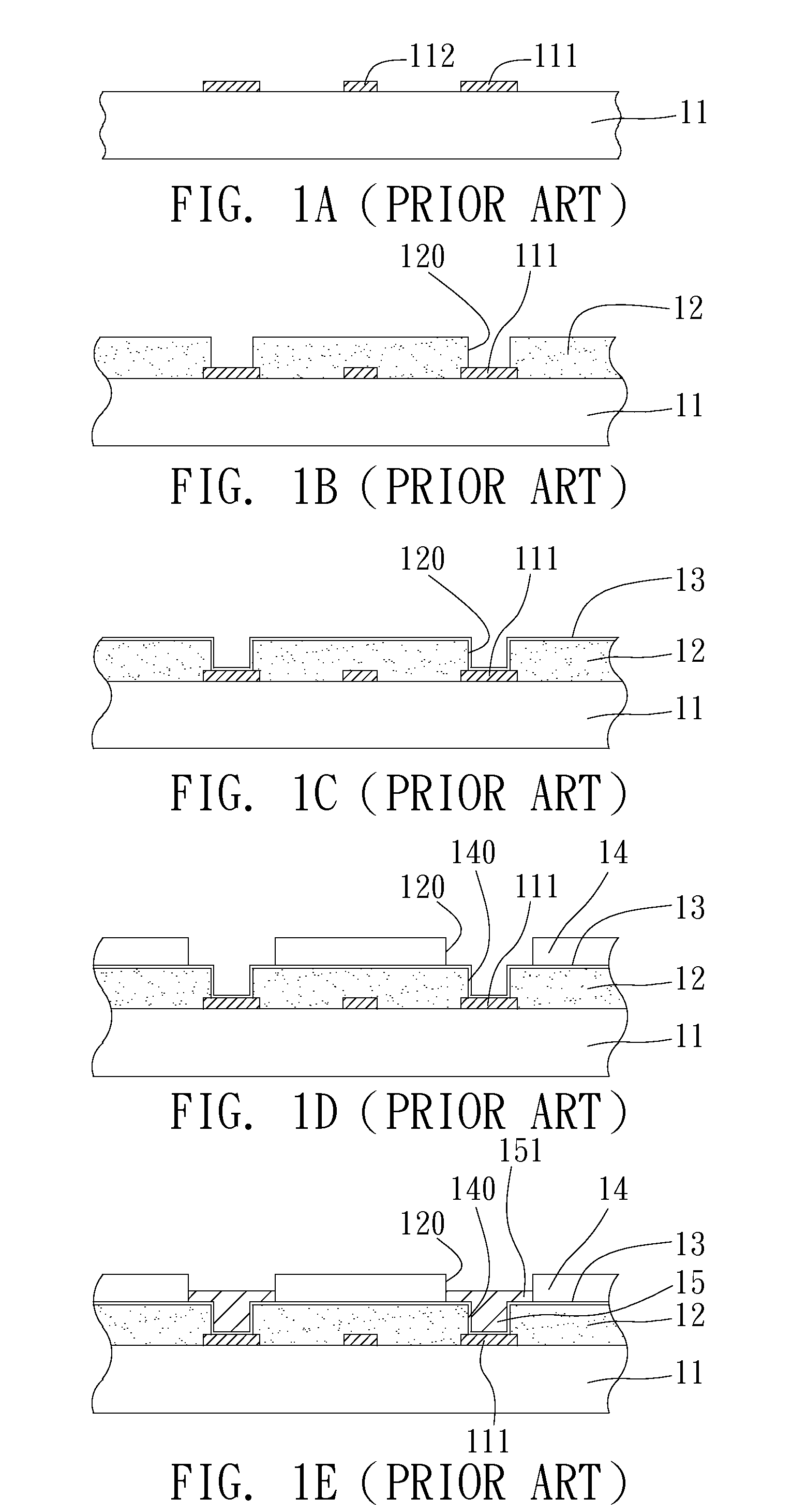
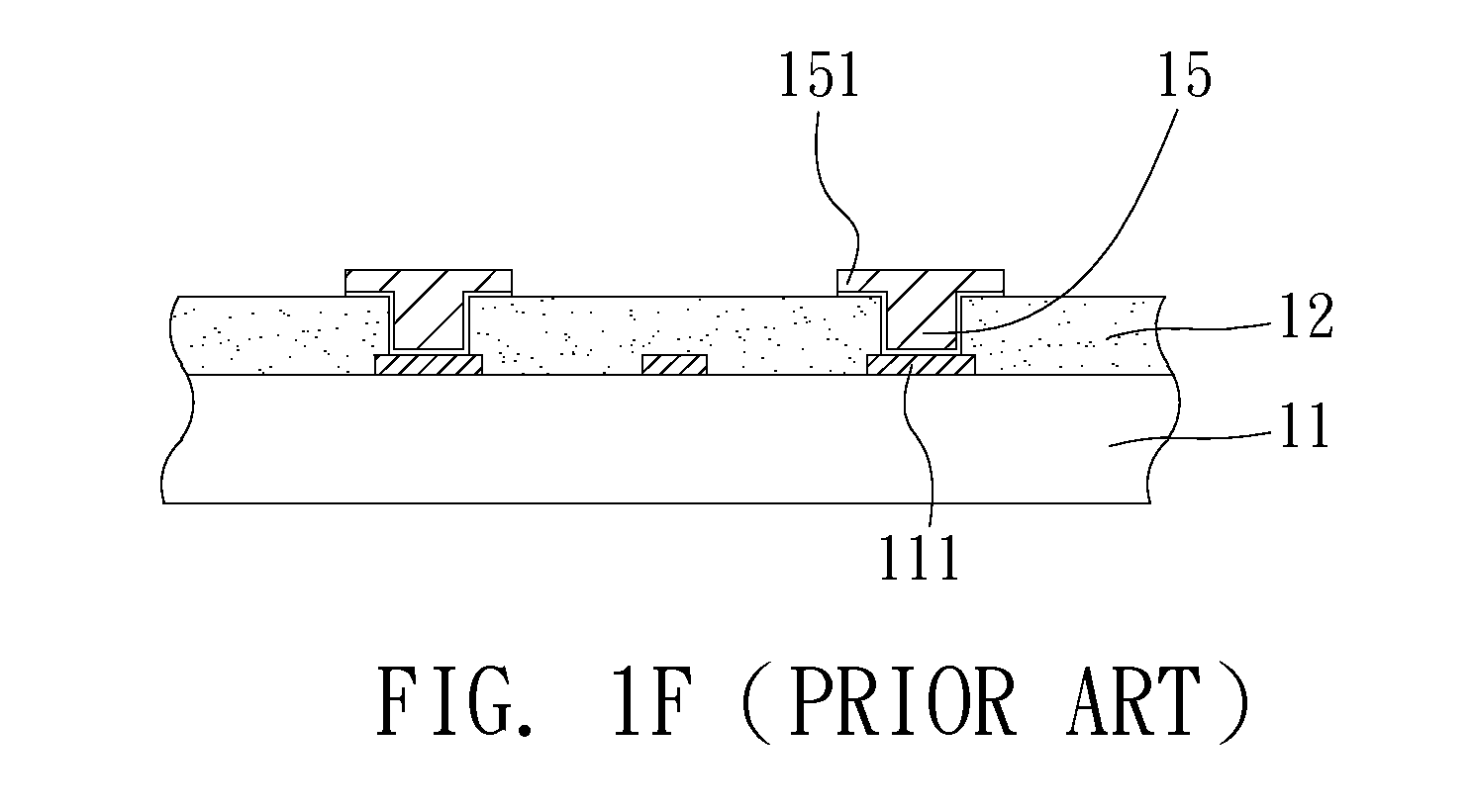
[0030]Referring to FIGS. 2A to 2J, a semiconductor package substrate structure and a manufacturing there according to a first embodiment of the present invention are depicted.

[0031]Referring to FIG. 2A, a substrate 20 with dielectric layer 21 formed on at least one surface thereof is first provided. A conductive layer 22 formed on the dielectric layer 21 is used as an electrical conduction path necessary in subsequent electroplating of metal materials. The conductive layer 22 can be formed from a metal or a plurality of metals deposited together and can be selected from a single layer or multiple layers of copper, tin, nickel, chromium, titanium, copper-chromium etc. It can also be formed from conductive polymers, such as polyacetylene, polyaniline or sulfuric organic polymer.

[0032]Referring to FIG. 2B, a first resist layer 23 is formed on the conductive layer 22 by printing, spin coating or adhesion. The first resist layer 23 undergoes a series of patterning steps (e.g. exposure, d...

second embodiment

[0046]Referring to FIGS. 3A and 3B, another manufacturing method of the present invention is shown. It is different from the previous embodiment in that the opaque region of the photomask completely covers all the electroplated conductive posts, including the areas between the electroplated conductive posts.

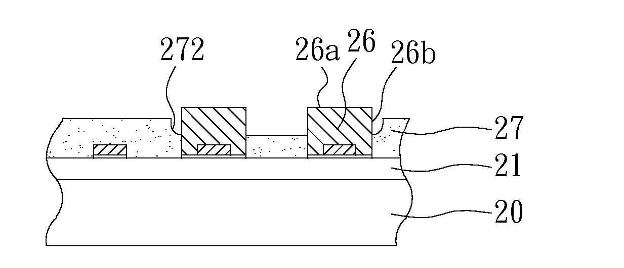
[0047]Referring to FIG. 3A, which is an equivalent to the stage of FIG. 2I in the first embodiment. The opaque region 281′ of the photomask 28 covers the electroplated conductive posts 26 and the areas between the electroplated conductive posts 26, and then the portions of the insulating protective layer 27 not masked by the opaque region 281 are exposed.

[0048]Referring to FIG. 3B, the unexposed portions of the insulating protective layer 27 are then removed, forming a revealing portion in the form of a recess 272 without penetrating the insulating protective layer 27 while exposing the tops 26a and a portion of the sides 26b of the various electroplated conductive posts. Thereaf...


PUM


Abstract

A semiconductor package substrate structure and a manufacturing method thereof are disclosed. The structure includes a substrate having a plurality of electrical connecting pads formed on at least one surface thereof; a plurality of electroplated conductive posts each covering a corresponding one of the electrical connecting pads and an insulating protective layer formed on the surface of the substrate and having a revealing portion for exposing the electroplated conductive posts therefrom. The invention allows the interval between the electroplated conductive posts to be minimized, the generation of concentrated stresses and the overflow of underfill to be avoided, as well as the reduction of the overall height of the fabricated package.

Description

FIELD OF THE INVENTION[0001]The present invention relates to a semiconductor package substrate structure and a manufacturing method thereof, and more particularly, to a semiconductor package substrate structure with electroplated conductive posts formed thereon and a manufacturing method thereof.BACKGROUND OF THE INVENTION[0002]In current flip-chip technology, there are electrode pads on an active face of a semiconductor chip in an integrated circuit (IC), while there are electrically connecting pads corresponding to the electrode pads on an organic circuit board. Solder structures or other conductive adhesives are formed between the electrode pads of the semiconductor chip and the electrically connecting pads of the circuit board, such that they provide electrical and mechanical connection therebetween. Related manufacturing processes are illustrated in FIGS. 1A to 1F as follows.[0003]Referring to FIG. 1A, a circuit board 11 with a plurality of electrically connecting pads 111 and ...

Claims


Application Information

Patent Timeline
IPC IPC(8): H01L23/52H01L21/00
CPCH01L23/498H01L24/11H01L23/49811H01L2924/14H01L2224/05568H01L2224/05023H01L2224/05001H01L2224/05111H01L2224/05147H01L2224/05155H01L2224/05166H01L2224/05171H01L2924/00014H01L2224/056H01L2224/05605H01L2224/05609H01L2224/05611H01L2224/05613H01L2224/05618H01L2224/0562H01L2224/05623H01L2224/05639H01L2224/05644H01L2224/05647H01L2224/05655H01L2224/05671H01L24/03H01L2924/00
Inventor HU, WEN-HUNG
Owner UNIMICRON TECH CORP
Why Eureka
Try Eureka