Display device

a display device and display technology, applied in the field of display devices, can solve the problems of increasing the number of output pins of the driver lsi, reducing the circuit area, and increasing the size of the frame area, so as to reduce the current consumption, and affect the effect of

Active Publication Date: 2008-11-13
PANASONIC LIQUID CRYSTAL DISPLAY CO LTD +1
View PDF6 Cites 17 Cited by
  • Summary
  • Abstract
  • Description
  • Claims
  • Application Information

AI Technical Summary

Benefits of technology

[0012]An advantage of the present invention is to provide an NMOS inverter that is less affected by manufacturing variations in the threshold voltage Vth of transistors or by the ON-resistance of the transistors, causes an output waveform to quickly rise and fall, and reduces current consumption.
[0013]According to an aspect of the present invention, a display area for displaying images and a drive circuit for driving the display area are provided on the same substrate. The drive circuit includes a level shifter circuit for increasing the amplitude of control clocks and an inverter circuit for generating inverted clocks to be provided to the level shifter.
[0014]The inverter circuit includes an input inverter having a high-resistance load and an output buffer having two transistors coupled in series. The inverter circu

Problems solved by technology

Also, a shrink effect produced by process miniaturization reduces the circuit area.
Therefore, disposition of a large number of control clock lines causes a problem that the size of the frame area is increased.
There also occurs another problem that the number of output pins of the driver LSI is increased and thus the cost of the driver LSI is increased.
However, the above-described inverter circuit has a problem that it is significantly affected by manufacturing variations of a threshold voltage Vth, since an input circuit of the inverter circuit employs a diode connection.
Specifically, the inverter circuit has a problem that a large Vt

Method used


Image

  • Display device
  • Display device
  • Display device

Examples


first embodiment

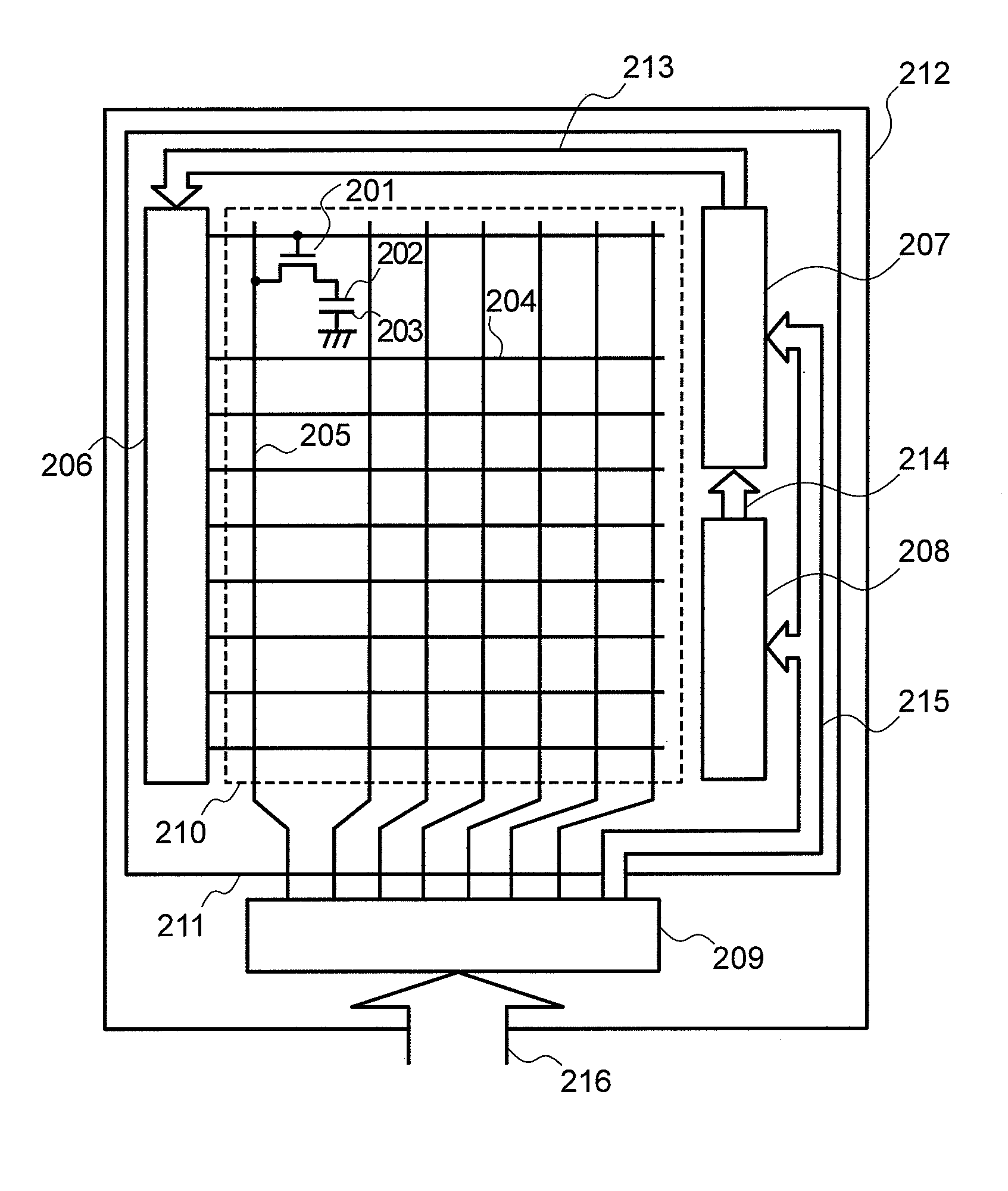
[0031]FIG. 1 is a block diagram showing a display device according to a first embodiment of the present invention. In FIG. 1, the display device according to this embodiment includes a liquid crystal panel 211 and a driver LSI 209 for driving the liquid crystal panel both provided on an insulating substrate 212. Disposed on the liquid crystal panel 211 in the horizontal direction and vertical direction are many gate lines 204 and many drain lines 205, respectively. Disposed at an intersection of each gate line 204 and each drain line 205 is a pixel, which includes a pixel electrode 202, a counter electrode 203, and a switching element 201. These components constitute a display area 210. Disposed on the periphery of the display area 210, that is, on the frame area are a power supply circuit 208, a level shifter circuit block 207, and a gate drive circuit 206.

[0032]The driver LSI 209 generates a control clock 215 to be provided to the power supply circuit 208 and level shifter circuit...

second embodiment

[0050]An inverter circuit according to a second embodiment of the present invention includes two output buffers. Thus, the inverter circuit is less affected by the CR time constant based on the resistance load R and a transistor parasite capacitance C included in the inverter circuit. Also, even if the resistance load R is increased, an output waveform of the inverter circuit rises and falls quickly. This embodiment will be described below with reference to FIGS. 5 and 6. The configuration of this embodiment except for that of the inverter circuit is the same as that of the first embodiment and will not be described.

[0051]FIG. 5 is a diagram showing a configuration of the inverter circuit according to this embodiment. In FIG. 5, the inverter circuit 302 includes an input inverter having the high-resistance load R and transistor Tr1, an intermediate buffer having the transistors Tr2 and Tr3, and an output buffer having transistors Tr4 and Tr5. The sources of the transistors Tr1, tR3,...

third embodiment

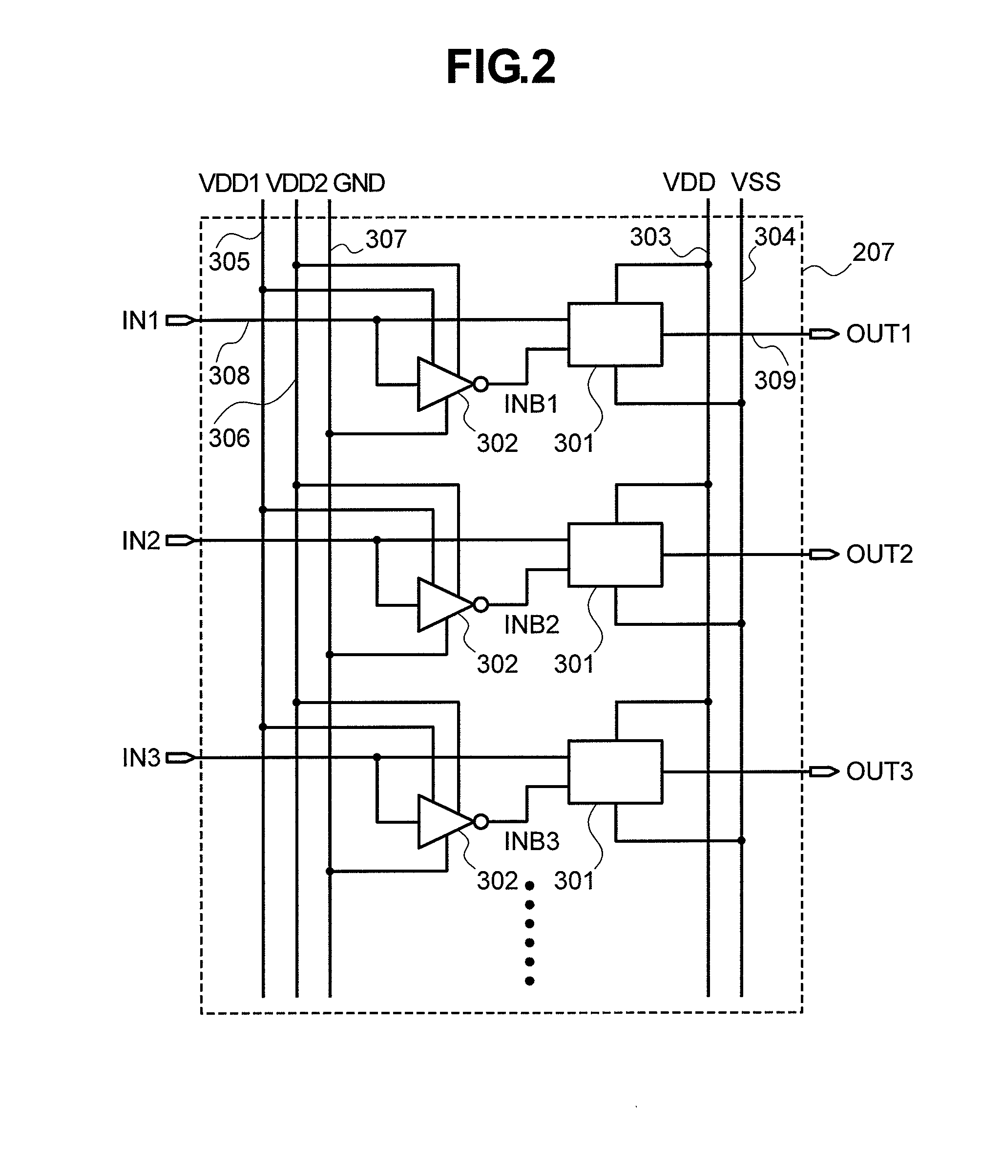
[0061]In an third embodiment of the present invention, the power supply voltage VDD of the level shifter circuit block 207 is used instead of the power supply voltage VDD1 that is a higher one of the power supply voltages used by the inverter circuit. This reduces the number of power supply voltages required to operate the integrated circuit, thereby reducing the number of control clocks of the integrated circuit.

[0062]FIG. 7 is a diagram showing a configuration of the level shifter circuit block 207 according to this embodiment. In FIG. 7, the level shifter circuit block 207 includes the level shifter circuit 301 for increasing the amplitude of a control clock outputted from the driver LSI 209 shown in FIG. 1 and the inverter circuit 302 for generating an inverted clock INB required to operate the level shifter circuit 301. The inverter circuit 302 is the same as that used in the first or second embodiment, so the configuration and operation thereof will not be described.

[0063]Acco...


PUM


Abstract

An inverter includes an input inverter having a high-resistance load and a first transistor and an output buffer including second and third transistors coupled in series. A power supply voltage is provided to satisfy an inequality VDD1>VDD2+Vth where VDD1 is the power supply voltage of the input inverter, VDD2 is the power supply voltage of the output buffer, and Vth is the threshold voltage of the transistors. Use of the high-resistance load allows an output waveform to rise and fall quickly, as well as reduces current consumption.

Description

CLAIM OF PRIORITY[0001]The present application claims priority from Japanese application serial no. 2007-106938 filed on Apr. 16, 2007, the content of which is hereby incorporated by reference into this application.BACKGROUND OF THE INVENTION[0002]1. Field of the Invention[0003]The present invention relates to a display device, in particular, a liquid crystal display device in which a drive circuit including an inverter circuit is integrated into a panel.[0004]2. Description of the Related Art[0005]Thin film transistor (TFT) liquid crystal display devices in which each pixel includes a switching element have widely been used as a display device of a personal computer or the like. Also, demand for TFT liquid crystal display devices as a display device of a small-size mobile terminal such as a cell phone has been grown. TFT liquid crystal display devices are required to achieve higher image quality and reduce power consumption, as well as strongly required to reduce the cost. In parti...

Claims


Application Information

Patent Timeline
IPC IPC(8): G02F1/136
CPCG09G3/3696G09G2300/0408G09G2310/0289
Inventor KAJIWARA, HISAYOSHIMAMBA, NORIOMIYAZAWA, TOSHIOMAKI, MASAHIRO
Owner PANASONIC LIQUID CRYSTAL DISPLAY CO LTD
Why Eureka
Try Eureka