Method of fabricating semiconductor memory device having self-aligned electrode, related device and electronic system having the same

a memory device and self-aligning technology, applied in semiconductor devices, digital storage, instruments, etc., can solve the problems of damage to the exposed difficulty in aligning the upper electrode on the phase change material layer, and inability to achieve high integration. , to prevent damage to the phase change pattern

Inactive Publication Date: 2008-11-13
SAMSUNG ELECTRONICS CO LTD
View PDF9 Cites 44 Cited by
  • Summary
  • Abstract
  • Description
  • Claims
  • Application Information

AI Technical Summary

Benefits of technology

[0013]One embodiment exemplarily described herein can be generally characterized as providing a method of fabricating a semiconductor memory device which is favorable for high integration and suitable for preventing damage to a phase change pattern.
[0014]Another embodiment exemplarily described herein can be generally characterized as providing a semiconductor memory device which is favorable for high integration and suitable for preventing damage to phase change pattern.
[0015]Still another embodiment exemplarily described herein can be generally characterized as providing a semiconductor memory device which is favorable for high integration and suitable for preventing damage to the phase change pattern.

Problems solved by technology

However, the photolithography process commonly causes alignment errors.
In this method, aligning the upper electrode on the phase change material layer is getting more difficult.
In this case, the exposed phase change material layer is damaged.
Damage to the phase change material layer deteriorates electrical characteristics of the phase change memory devices.
In this method, however, the upper electrode is an obstacle to the high integration of the phase change memory device.

Method used


Image

  • Method of fabricating semiconductor memory device having self-aligned electrode, related device and electronic system having the same
  • Method of fabricating semiconductor memory device having self-aligned electrode, related device and electronic system having the same
  • Method of fabricating semiconductor memory device having self-aligned electrode, related device and electronic system having the same

Examples


Embodiment Construction

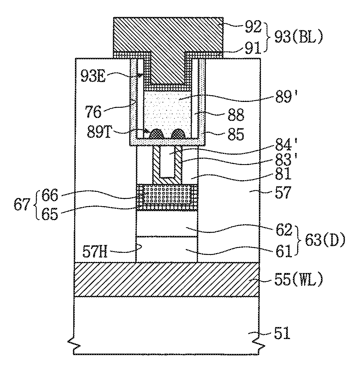
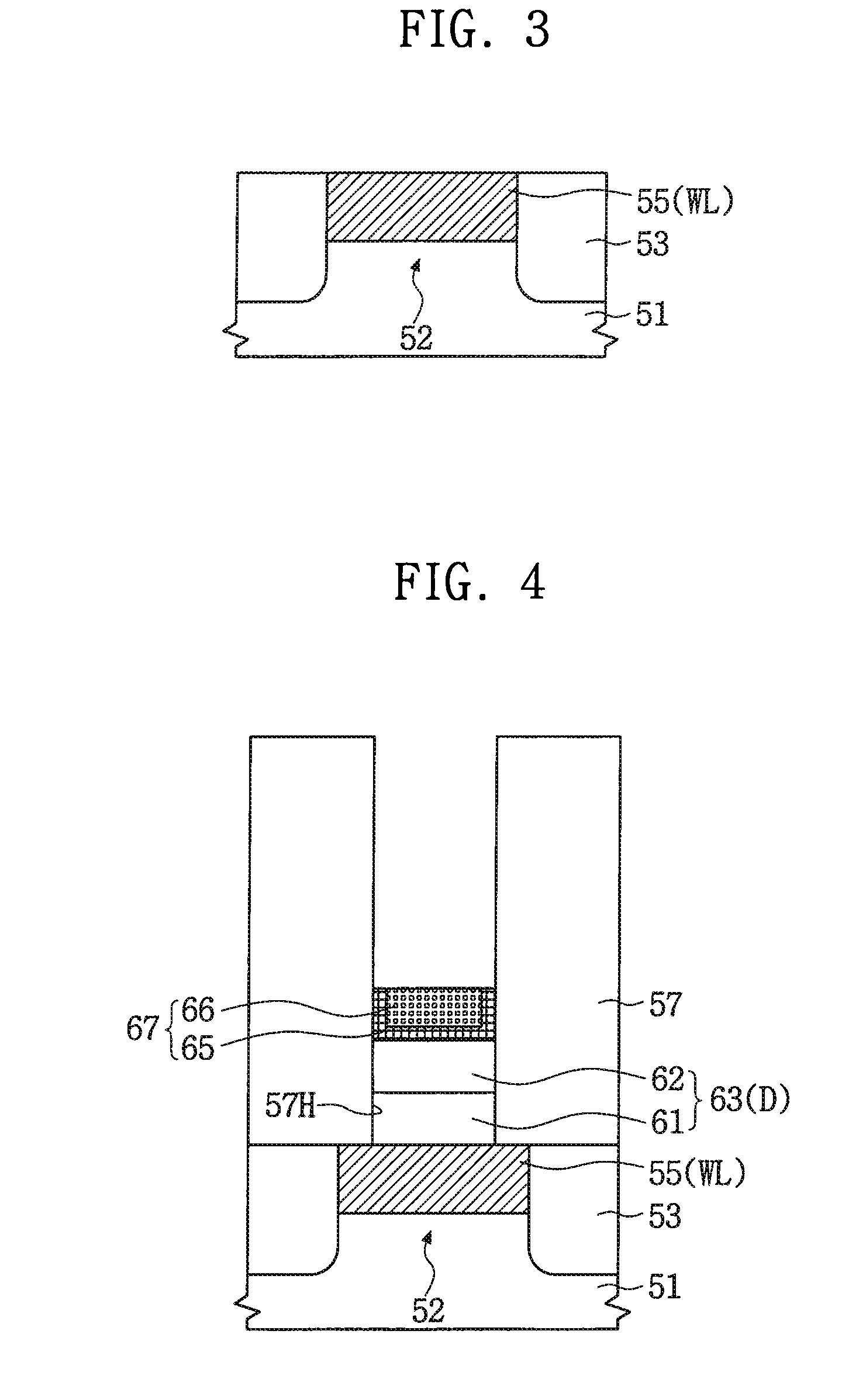
[0036]Exemplary embodiments of the present invention will now be described with reference to the accompanying drawings. These embodiments may, however, be realized in different forms and should not be construed as limited to the embodiments set forth herein. Rather, these embodiments are provided so that this disclosure will be thorough and complete, and will fully convey the scope of the invention to those skilled in the art. In the drawings, the thickness of layers and regions are exaggerated for clarity. In addition, when a layer is described to be formed on another layer or on a substrate, it means that the layer may be formed on the other layer or on the substrate, or a third layer may be interposed between the layer and the other layer or the substrate. Like numbers refer to like elements throughout the specification.

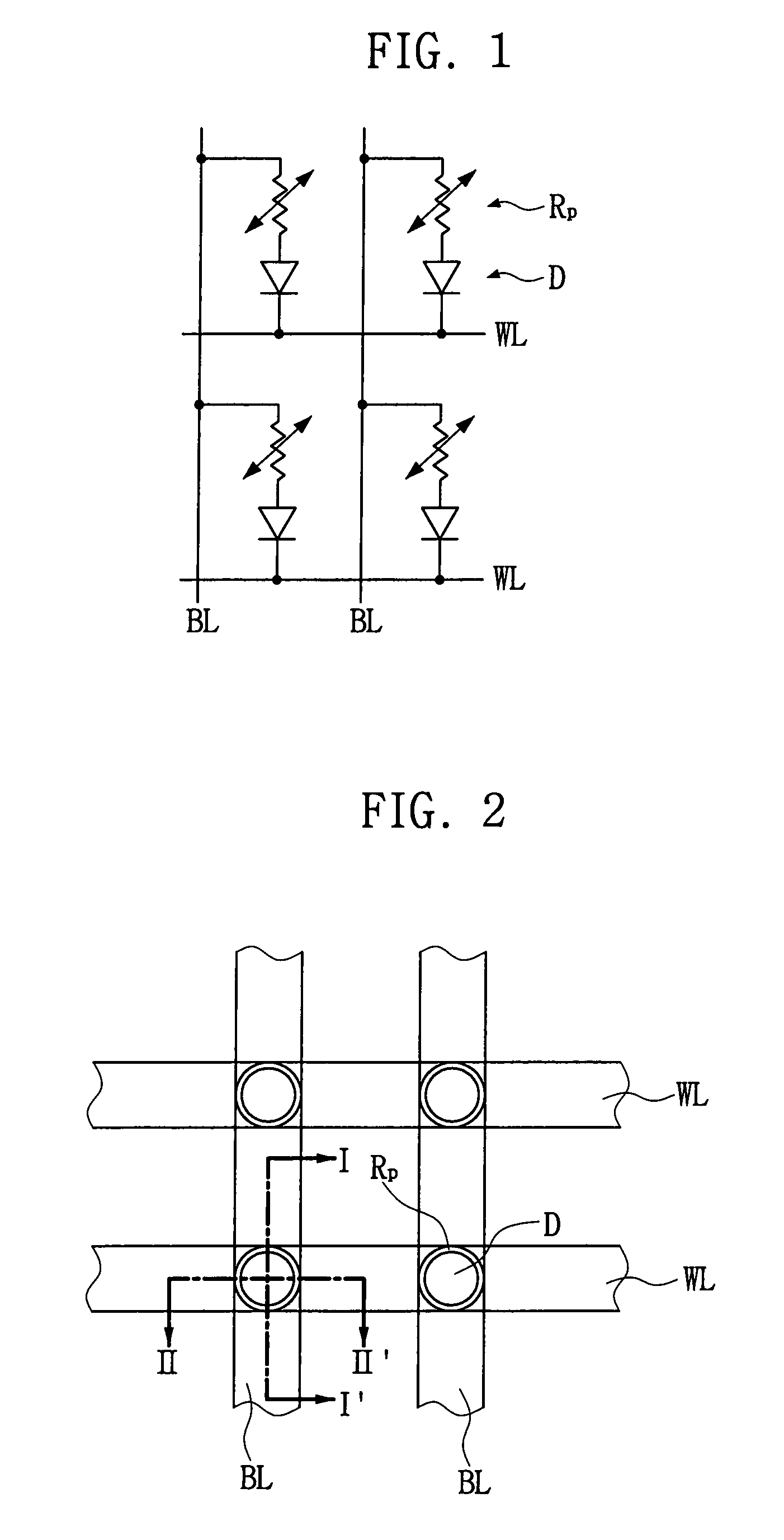
[0037]FIG. 1 is an equivalent circuit diagram illustrating a part of a cell array region of a semiconductor memory device according to first to fourth exemplary e...


PUM


Abstract

A method of fabricating a semiconductor memory device having a self-aligned electrode is provided. An interlayer insulating layer having a contact hole is formed on a substrate. A phase change pattern partially filling the contact hole is formed. A bit line which includes a bit extension self-aligned to the phase change pattern and crosses over the interlayer insulating layer is formed. The bit extension may extend in the contact hole on the phase change pattern. The bit extension contacts the phase change pattern.

Description

CROSS-REFERENCE TO RELATED APPLICATION[0001]This application claims the benefit of Korean Patent Application No. 10-2007-0045164, filed May 9, 2007, the disclosure of which is hereby incorporated herein by reference in its entirety.BACKGROUND[0002]1. Field of Invention[0003]Exemplary embodiments of the present invention relate generally to semiconductor devices and methods of fabricating the same and, more particularly, to a method of fabricating a semiconductor memory device having an electrode which is self-aligned to a phase change pattern, and the related device.[0004]2. Description of the Related Art[0005]Semiconductor memory devices may be classified into volatile memory devices and non-volatile memory devices. Non-volatile memory devices do not lose data stored therein even if power supply is interrupted. Accordingly, the non-volatile memory devices are widely applied to secondary storage devices of mobile communication systems, portable memory devices and all kinds of digita...

Claims


Application Information

Patent Timeline
Patent Type & Authority Applications(United States)
IPC IPC(8): H01L47/00
CPCH01L27/2409H01L27/2436H01L45/06H01L45/1233H01L45/1273H01L45/141H01L45/1683H10B63/20H10B63/30H10N70/231H10N70/8418H10N70/882H10N70/826H10N70/066G11C13/0004
Inventor KIM, JUNG-INOH, JAE-HEEKONG, JUN-HYOKPARK, JAE-HYUNLEE, KWANG-WOO
Owner SAMSUNG ELECTRONICS CO LTD
Why Eureka
Try Eureka