Manufacturing method of liquid crystal display

a liquid crystal display and manufacturing method technology, applied in the field of manufacturing a transflective display device, can solve the problems of long manufacturing time and high manufacturing cost, low and inability to induce appropriate diffused reflection and scattering, etc., to achieve the effect of simplifying manufacturing processes and enhancing the yield and reflection efficiency of concavo-convex pattern

Inactive Publication Date: 2008-11-20
SAMSUNG DISPLAY CO LTD
View PDF16 Cites 6 Cited by
  • Summary
  • Abstract
  • Description
  • Claims
  • Application Information

AI Technical Summary

Benefits of technology

[0012]Accordingly, it is an aspect of the present invention to provide a method for manufacturing a display device that is capable of enhancing the yield and reflection efficiency of concavo-convex patterns and simplifying manufacturing processes.

Problems solved by technology

The half exposure method entails performing a photolithography process multiple times to form the concavo-convex patterns, contact holes, etc., and thus requires long manufacturing time and high manufacturing cost.
As for methods using the slit mask, they cannot induce appropriate diffused reflection and scattering since the yield and reflection efficiency of the concavo-convex patterns are low.

Method used


Image

  • Manufacturing method of liquid crystal display
  • Manufacturing method of liquid crystal display
  • Manufacturing method of liquid crystal display

Examples


first embodiment

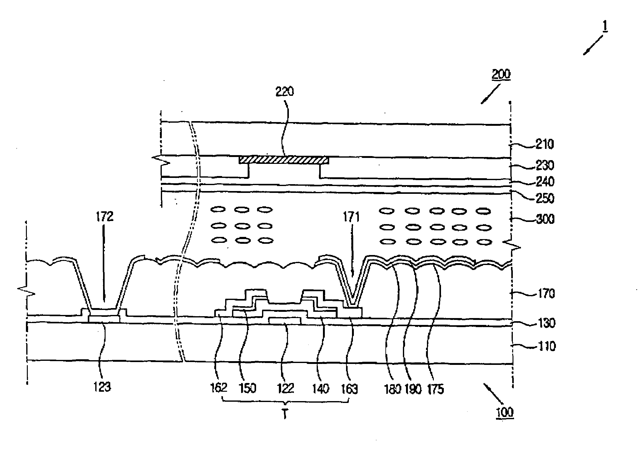
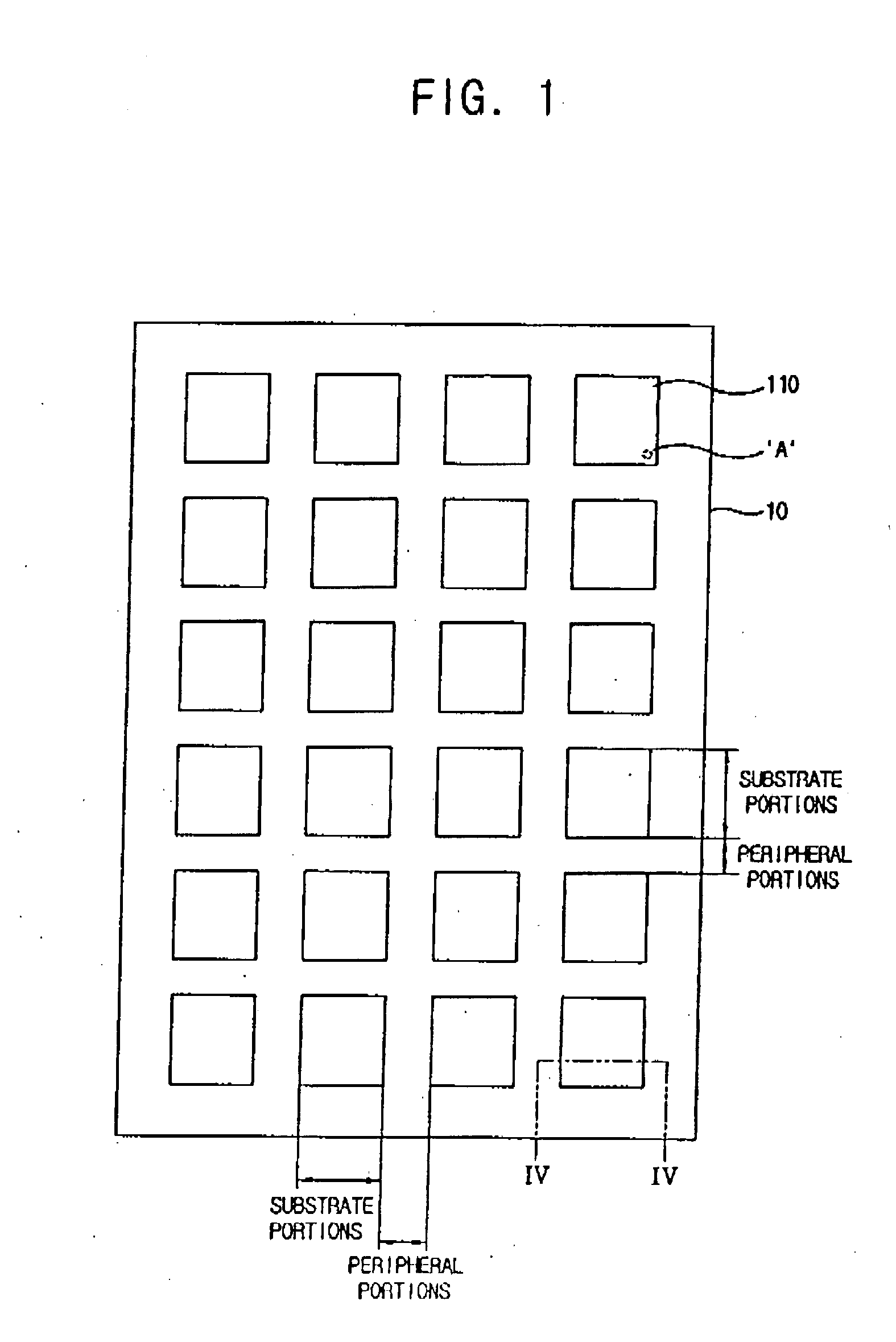
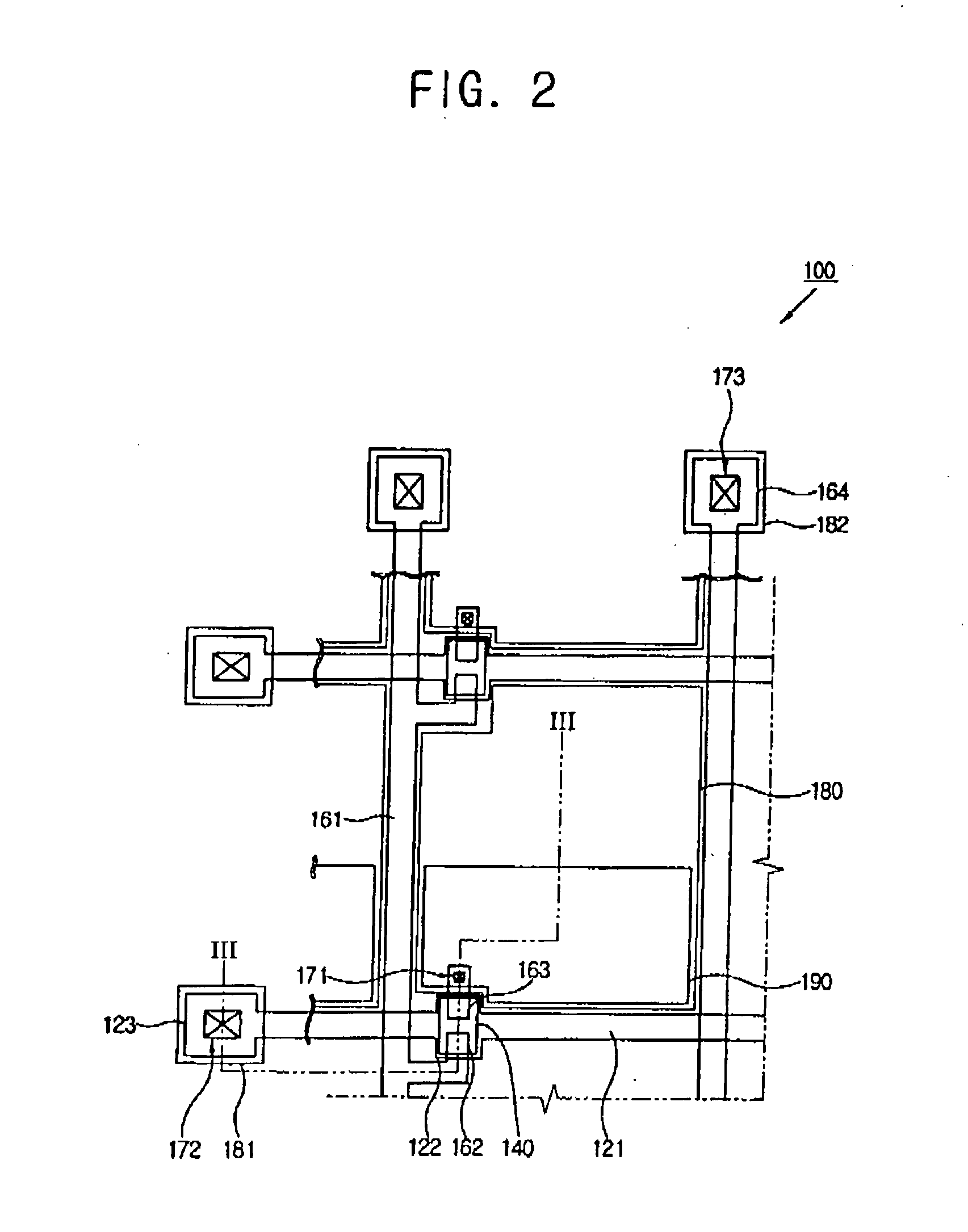
[0024]FIG. 1 is a plan view illustrating a mother substrate substance according to the present invention, FIG. 2 is a layout of the area ‘A’ marked in FIG. 1, and FIG. 3 is a cross-sectional view cut along the dotted line III-III of FIG. 2.

[0025]Referring to FIGS. 1, 2 and 3, a liquid crystal panel 1 according to a first embodiment of the present invention includes a thin film transistor substrate (first substrate) 100, color filter substrate (second substrate) 200, and a liquid crystal layer 300 positioned between the first substrate 100 and the second substrate 200.

[0026]First, the thin film transistor substrate 100 will be described below.

[0027]As shown in FIG. 1, a plurality of first substrates 100 are manufactured from a large mother substrate substance 10 by a well-known thin film transistor substrate manufacturing process. Although FIG. 1 illustrates that 24 insulating substrates 110 can be made from the mother substrate substance 10, this is an example and not meant to be li...

second embodiment

[0062]The small-molecule organic layer is hardened by ultraviolet radiation or heat treatment. In the second embodiment, the mold 400 has a concavo-convex pattern 410 in the areas that will be aligned with a pixel area or a substrate area. In addition, the mold 400 has a protection film removing portion 420 positioned to align with the peripheral area of the mother substrate substance 10. The protection film removing portion 420 is extruded toward the organic passivation layer 170. Preferably, as shown in FIG. 5B, the protection film removing portion 420 is formed with a predetermined height so that it comes in contact with the insulating substrate 110 when the mold 400 is pressurized in the direction shown by the arrows. Here, in order to harden the organic passivation layer 170 while maintaining the concavo-convex pattern 175, the mold 400 is preferably made of a transparent material that can transmit ultraviolet radiation. The transparent material used for forming the mold 400 ma...


PUM


Abstract

A method of manufacturing a liquid crystal display at a reduced cost is presented. The method entails: preparing an insulating substrate; forming a gate line and a data line on the insulating substrate to define a pixel area; forming a thin film transistor at an intersection of the gate line and the data line; forming A passivation layer on the thin film transistor; positioning a mold having a concavo-convex pattern on the organic passivation layer, pressing the mold, and forming the concavo-convex pattern on the surface of the organic passivation layer. A pixel electrode on the organic passivation layer is formed.

Description

CROSS-REFERENCE TO RELATED APPLICATIONS[0001]This application claims priority from Korean Patent Application No. 2005-006456 filed on Jul. 19, 2005 in the Korean Intellectual Property Office, the disclosure of which is incorporated herein by reference.BACKGROUND OF INVENTION[0002]1. Field of Invention[0003]The present invention relates to a manufacturing a transflective display device.[0004]2. Description of the Related Art[0005]Recently, display devices such as the liquid crystal display (LCD) device, plasma display panel (PDP), organic light emitting diode (OLED), and electro phoretic indication display, among others, have been gradually replacing the cathode ray tube (CRT) in various display applications.[0006]A liquid crystal display includes a thin film transistor substrate on which thin film transistors are formed, color filter substrate on which color filters are formed, and a liquid crystal panel having liquid crystal layers inserted between the thin film transistor substrat...

Claims


Application Information

Patent Timeline
Patent Type & Authority Applications(United States)
IPC IPC(8): H01L21/70
CPCG02F1/133555G02F1/13439G02F2001/133776G03F7/0007G02F1/133504G02F1/133776G02F1/1335G02F1/136
Inventor CHANG, JAE-HYUKROH, NAM-SEOKHONG, MUN-PYOPARK, DAE-JIN
Owner SAMSUNG DISPLAY CO LTD
Why Eureka
Try Eureka