Method for manufacturing semiconductor device including etching process of silicon nitride film

Inactive Publication Date: 2008-11-27
NEC ELECTRONICS CORP
View PDF3 Cites 116 Cited by
  • Summary
  • Abstract
  • Description
  • Claims
  • Application Information

AI Technical Summary

Benefits of technology

[0022]Thus, since the arsenic-containing region is removed by dry etching and the rest of the region is remov

Problems solved by technology

However, when the silicon nitride film is removed, arsenic included in the silicon nitride film is eluted into the wet etching liquid.
Particles acting as dust create wiring short circuits, pattern formation anomalies, and deterioration of the tolerance of the insulating film, etc. and cause a decrease in the yield of the semiconductor product and its reliability and deterioration in the performance.
In other words, since there is a danger

Method used


Image

  • Method for manufacturing semiconductor device including etching process of silicon nitride film
  • Method for manufacturing semiconductor device including etching process of silicon nitride film
  • Method for manufacturing semiconductor device including etching process of silicon nitride film

Examples


first embodiment

[0100]The present invention relates to an etching technique of a silicon nitride film in a manufacturing process of a semiconductor device by combining a first etching process where a arsenic-containing region is removed by dry etching using a second etching process where the rest of the region is removed by wet etching when the silicon nitride film including arsenic in the upper part is removed. Then, in the first embodiment of the present invention, the concept of the present invention will be explained using a manufacturing process as an example where selective implantation is performed using the silicon nitride film as a mask and an N-type diffusion region is formed over a silicon substrate.

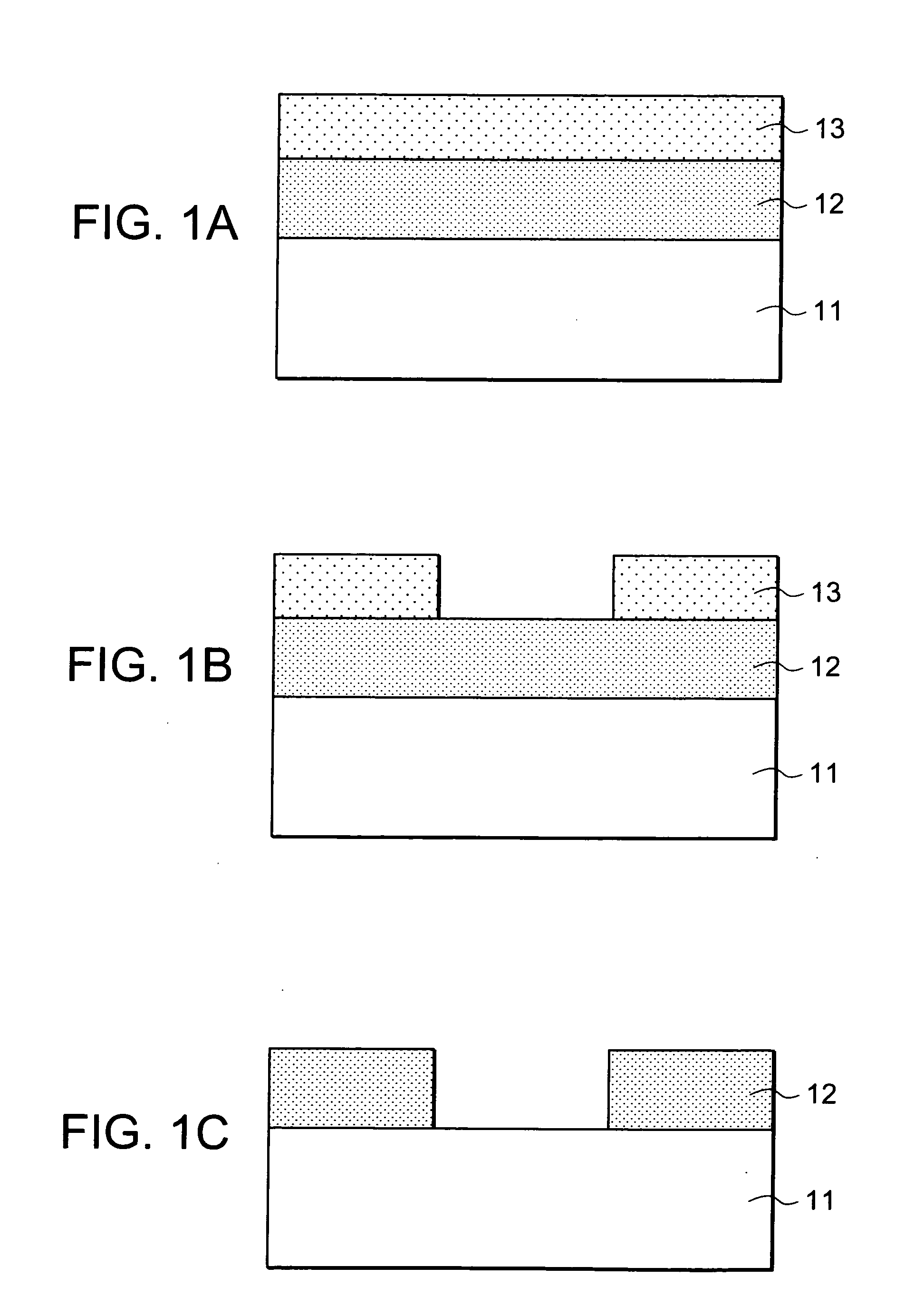
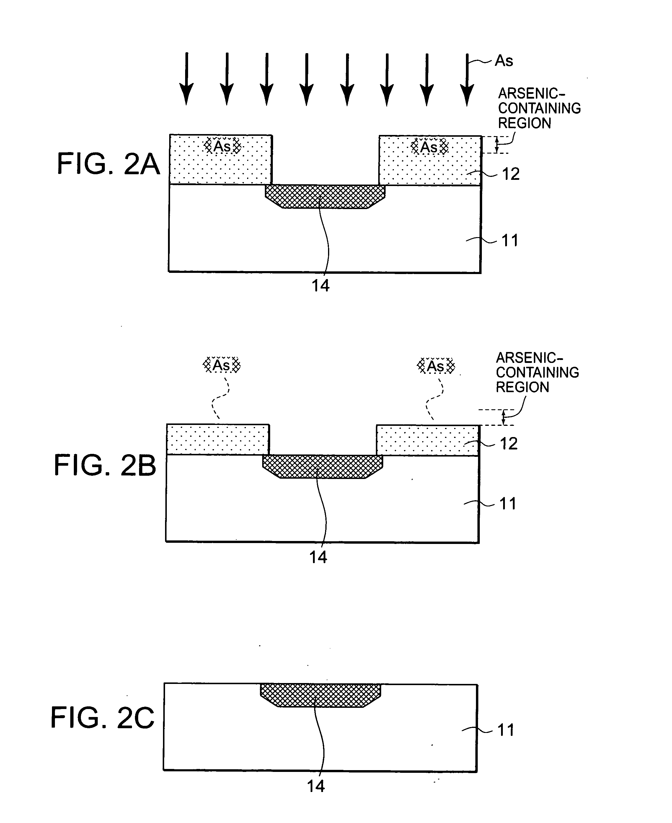
[0101]FIGS. 1 and 2 are cross-sectional drawings illustrating a manufacturing method of a semiconductor device, step by step, which has an N-type diffusion region related to the first embodiment.

[0102]First, as shown in FIG. 1A, a silicon nitride film 12 is formed over a silicon substrate 11 ...

second embodiment

[0116]Next, the present invention is illustrated by using the following examples. In the second embodiment of the present invention, an example of a manufacturing method for a memory cell transistor of a split-gate type nonvolatile memory which is a kind of electrically erasable nonvolatile semiconductor memory device.

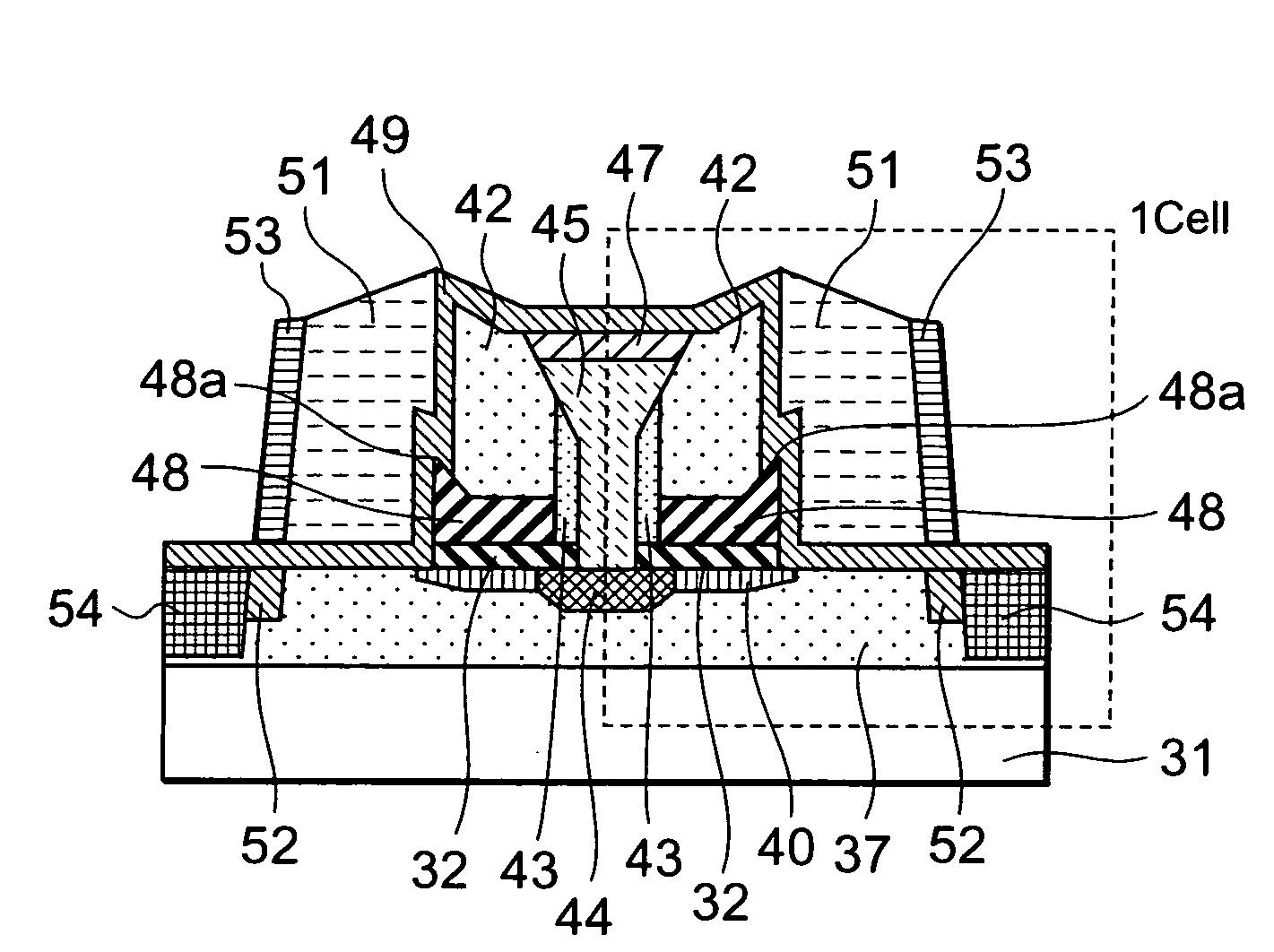
[0117]FIG. 3A is a cross-sectional drawing illustrating a structure of a memory cell transistor of the second embodiment, and FIG. 3B is a plane drawing (plane layout) as seen from above. The cross-sectional drawing of FIG. 3A corresponds to the cross-section at A-A′ in FIG. 3B. Moreover, FIG. 3A and FIG. 3B illustrate two memory cell transistors in which the memory cell transistors are arranged symmetrically relative to the common plug 45. The part surrounded by the dotted line corresponds to one memory cell transistor (1 cell) and a memory of one bit of data is possible.

[0118]As shown in FIG. 3, a P well 37 which is a P-type well, a first source / drain diffusion regio...

third embodiment

[0161]In the third embodiment of the present invention, an example will be explained in which the invention is utilized in the process for removing the silicon nitride film-mask which becomes unnecessary after the process for introducing arsenic ions into the field oxide film (isolation region) in a manufacturing method of a Metal Oxide Semiconductor (MOS) transistor having a silicide structure disclosed in JP-A-1998-50636.

[0162]Describing it as a precaution, in the third embodiment, the object into which arsenic is selectively injected is different from those in the first embodiment and the second embodiment, and it is not the semiconductor substrate (silicon substrate) itself but the insulating film (field oxide film) formed over the semiconductor substrate. Specifically, the object into which arsenic is injected depends on for what purpose the selective implantation of arsenic is performed. In the present invention, the object into which arsenic is injected is not limited to the ...


PUM


Abstract

A manufacturing method of a semiconductor device includes the step for forming a silicon nitride film having a first part where arsenic is included and a second part where less amount of or substantially no arsenic is included, the step for removing at least a portion of the first part by dry etching, and the step for removing at least a portion of the second part by wet etching. Since arsenic in the silicon nitride film is removed by dry etching, arsenic is never eluted into the wet etching liquid from the silicon nitride film during subsequent wet etching. Therefore, one can prevent the wet etching from being contaminated. Etching of the silicon nitride film is performed by a combination of dry etching and wet etching. Therefore, compared with the case where etching is performed only by dry etching, plasma damage to the region exposed in the plasma atmosphere except for the silicon nitride film can be decreased.

Description

BACKGROUND OF THE INVENTION[0001]1. Field of the Invention[0002]The present invention relates to a method for manufacturing a semiconductor device and, specifically, relates to a method for manufacturing a semiconductor device which includes a step for etching a silicon nitride film containing arsenic.[0003]2. Description of Related Art[0004]In a processing technology of a semiconductor device, an impurity diffusion technology for introducing impurities is used in order to have suitable conductivity and characteristics by mixing N-type and P-type impurities.[0005]The impurity diffusion technology includes an ion implantation technique in which impurities such as boron (B), arsenic (As), and phosphorus (P) are ionized; high energy is imparted to the ionized impurities by an accelerating voltage to make them collide with the surface of the semiconductor. Moreover, selective implantation is performed when the impurities are injected only into a desired region. This selective implantati...

Claims


Application Information

Patent Timeline
IPC IPC(8): H01L21/336H01L21/28
CPCH01L21/28273H01L21/31111H01L21/31116H01L21/823842H01L21/823878H01L27/11519H01L29/42324H01L29/66825H01L29/7885H01L29/40114H10B41/10
Inventor KOJIMA, TATSUKITSUJITA, KENJI
Owner NEC ELECTRONICS CORP
Why Eureka
Try Eureka