LED device having improved light output

a technology of led devices and light output, applied in the direction of discharge tubes/lamp details, organic semiconductor devices, discharge tubes luminescnet screens, etc., can solve the problems of difficult patterned deposition, low light output efficiency, and high cost of metal masks, so as to improve the efficiency of light output and improve the sharpness of pixellated led devices. , the effect of increasing the uniformity of light outpu

Active Publication Date: 2008-12-04
GLOBAL OLED TECH
View PDF20 Cites 47 Cited by
  • Summary
  • Abstract
  • Description
  • Claims
  • Application Information

AI Technical Summary

Benefits of technology

[0020]The present invention has the advantage that it increases the uniformity of light output and the efficiency of light output from an LED device and improves the sharpness of a pixellated LED device.

Problems solved by technology

However, patterned deposition is difficult, requiring, for example, expensive metal masks.
However, such designs are relatively inefficient, since approximately two-thirds of the light emitted may be absorbed by the color filters.
It has been found that one of the key factors that limits the efficiency of LED devices is the inefficiency in extracting the photons generated by the electron-hole recombination out of the LED devices.
Due to the relatively high optical indices of the EML and transparent electrode materials used, most of the photons generated by the recombination process are actually trapped in the devices due to total internal reflection.
In general, up to 80% of the light may be lost in this manner.
In any of these LED structures, the problem of trapped light remains.
However, none of these approaches cause all, or nearly all, of the light produced to be emitted from the device.
However, scattering techniques, by themselves, may cause light to pass through the light-absorbing material layers multiple times where they are absorbed and converted to heat.
Moreover, trapped light may propagate a considerable distance horizontally through the cover, substrate, or organic layers before being scattered out of the device, thereby reducing the sharpness of the device in pixellated applications such as displays.
The particular arrangements, however, may still result in reduced sharpness of the device.
However, many electrode materials that are transparent, such as ITO, have low conductivity, which results in a voltage drop across the display.
This in turn causes variable light output from the light emitting elements in the display, resistive heating, and power loss.
This results in incident light reflecting off the auxiliary electrode and thereby reducing the overall contrast ratio of the display.
This makes the display less effective for use under high ambient light conditions, such as outdoors under bright sunshine.
However, such an arrangement does not improve the distribution of current within light-emitting areas.
For devices, such as area illumination lamps that are expected to have large, light-emitting areas, such a solution is helpful but may not be adequate.
However, this solution likewise does not improve the distribution of current within the light-emitting area.
The employment of a light-scattering layer on the substrate or cover of an LED device, as taught in the prior art, does not address this problem.
Moreover, these prior-art LED devices require a transparent electrode having limited conductivity that further reduces light output and decreases the uniformity of the light output.
Prior-art solutions such as auxiliary electrodes above or below a transparent electrode do not address the problem of conductivity within a light-emitting area.

Method used


Image

  • LED device having improved light output
  • LED device having improved light output
  • LED device having improved light output

Examples


Embodiment Construction

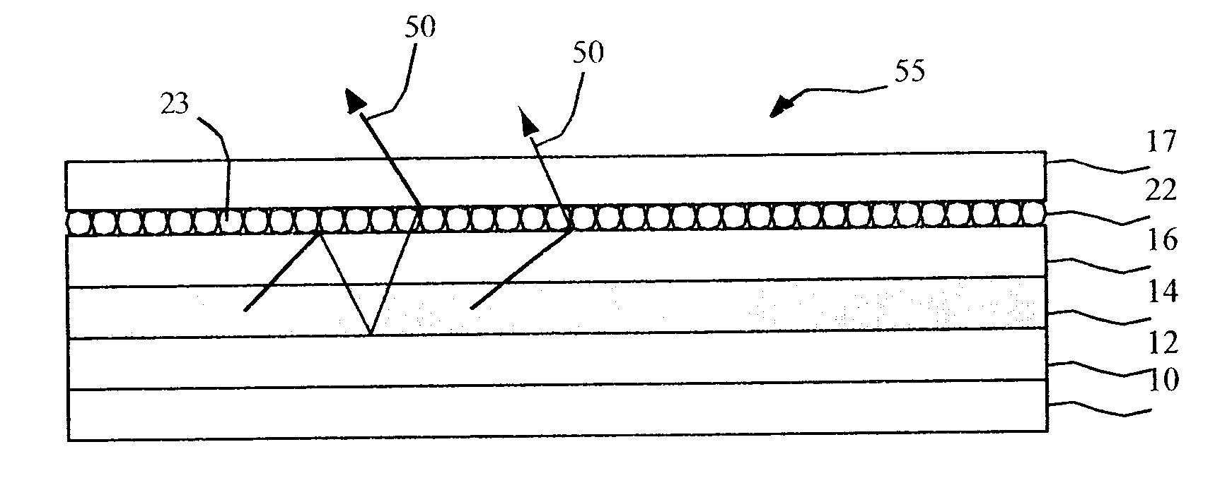
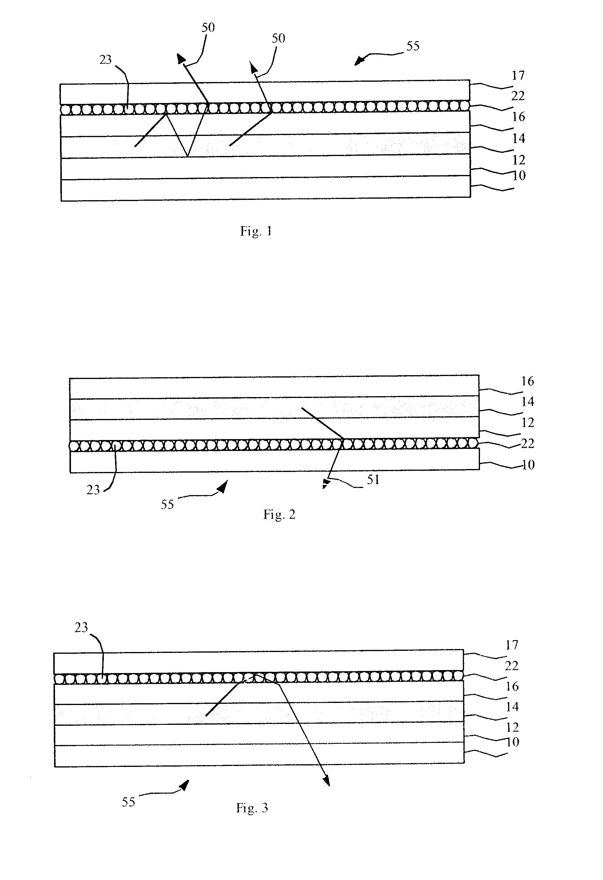
[0031]Referring to FIG. 1, in accordance with one embodiment of the present invention, a light-emitting device comprises a substrate 10, a first electrode 12 formed over the substrate 10, a light-emitting layer 14 formed over the first electrode 12, a second electrode 16 formed over the light-emitting layer 14, wherein at least one of the first and second electrodes 12, 16 is transparent; and a light-scattering layer 22 comprising electrically conductive, light-scattering particles 23 in physical and electrical contact with the first or second electrode 12, 16. The light-scattering layer 22 is formed on a side of the first or second electrode 12, 16, and opposite the light-emitting layer 14.

[0032]In various embodiments of the present invention, the light-emitting layer 14 comprises organic materials, for example, those employed in OLED devices. Alternatively inorganic light-emitting particles, for example, core / shell quantum dots in a semiconductor matrix, as taught in co-pending, c...


PUM


Abstract

A light-emitting device, including a substrate and a first electrode formed over the substrate. A light-emitting layer is formed over the first electrode. A second electrode is formed over the light-emitting layer. At least one of the first and second electrodes is transparent. A light-scattering layer comprising electrically-conductive, light-scattering particles is located in physical and electrical contact with the first or second electrode. The light-scattering layer is formed on a side of the first or second electrode, and opposite the light-emitting layer.

Description

FIELD OF THE INVENTION[0001]The present invention relates to light-emitting diode (LED) devices, and more particularly, to LED device structures for improving light output and lifetime of LED devices.BACKGROUND OF THE INVENTION[0002]Light-emitting diodes (LEDs) are a promising technology for flat-panel displays and area illumination lamps. The technology relies upon thin-film layers of organic or inorganic materials coated upon a substrate. Organic LED devices generally can have two formats known as small molecule devices such as disclosed in U.S. Pat. No. 4,476,292, issued Oct. 9, 1984 to Ham et al., and polymer OLED devices such as disclosed in U.S. Pat. No. 5,247,190, issued Sep. 21, 1993 to Friend et al. Alternatively, inorganic LED devices are known that employ quantum dots. Either type of LED device may include, in sequence, at least an anode, a light-emitting layer (EML), a cathode and an EL element. The EL element disposed between the anode and the cathode may also include a...

Claims


Application Information

Patent Timeline
Patent Type & Authority Applications(United States)
IPC IPC(8): H05B33/00B05D5/12
CPCB82Y20/00B82Y30/00H01L51/5012H01L51/5268H01L2251/5369H01L2933/0091H05B33/22H10K50/11H10K50/854H10K2102/331
Inventor COK, RONALD S.
Owner GLOBAL OLED TECH
Why Eureka
Try Eureka