

Semiconductor apparatus and method for fabricating the same
a technology of semiconductor devices and electrodes, applied in the direction of semiconductor devices, electrical devices, basic electric elements, etc., can solve the problems of short channel effect, deterioration of cross sectional shape of trenches, and deterioration of i>a/i>, so as to reduce the amount of burrs, efficiently remove or reduce the remaining burrs, and prevent the effect of electric field concentration in the trench upper portion
- Summary
- Abstract
- Description
- Claims
- Application Information
AI Technical Summary
Benefits of technology
Problems solved by technology
Method used
Image

Examples
examples
[0135]Next, Examples of the present invention will be described in detail.
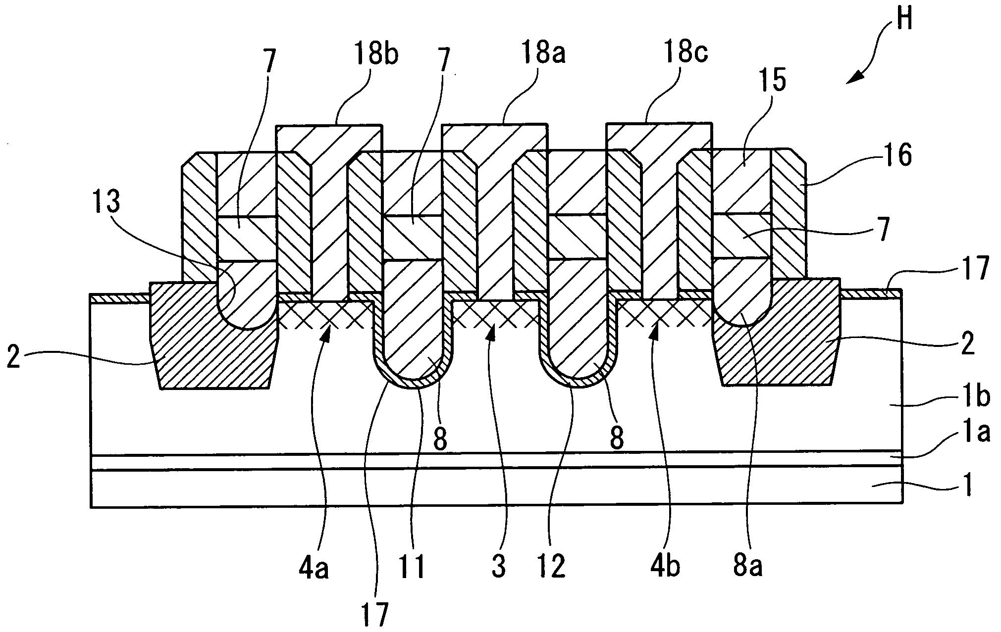
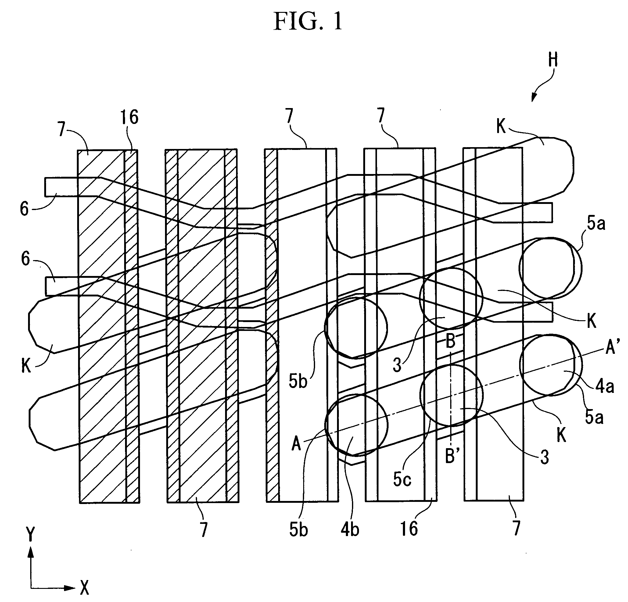
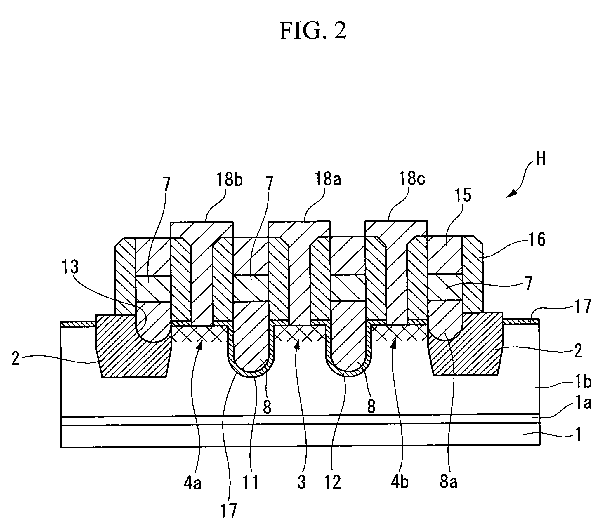
[0136]A semiconductor apparatus H shown in FIGS. 1 and 2 was produced by the steps shown in FIGS. 4 to 12.
examples 1 and 2
[0137]Optimal conditions for a hydrogen baking treatment and an oxidation treatment were studied and with respect to the sample in which the Si burr was generated after subjecting trenches to a silicon dry etching process, optimal conditions for a light hydrogen baking treatment and a light DCE oxidation treatment were examined.
[0138](Sample Structure)
[0139]The sample shape after the dry etching process was like the one shown in FIG. 5.
[0140](Dry Etching Apparatus)
[0141]A commercially available ICP plasma etching apparatus was used.
[0142](Conditions for Silicon Dry Etching Process)
[0143]Conditions were: HBr / Cl2 / O2=100 / 90 / 10 sccm, 10 mTorr (1.33 Pa), and RF (upper portion / lower portion)=500 W / 100 W (stage temperature=10° C.).
[0144](Standard Conditions for Hydrogen Baking Treatment)
[0145]Conditions were: H2=15 L / min, 20 Torr (2.67×10³ Pa), 850° C., and 60 seconds.
[0146]The condition necessary for the hydrogen baking treatment was to satisfy both the following two requirements:[0147](1...
example 3
[0156]Next, optimal conditions in terms of temperature and time with respect to the most effective DCE oxidation treatment were examined. In order to avoid depositing oxide film on the Si burr portion, the temperature was adjusted to 850° C., which was the lower limit set in the apparatus used, and the optimal time condition (50, 100, 150, and 200 seconds) was examined here. The upper film thickness a′, the intermediate film thickness b′, and the bottom film thickness c′ were measured, and their ratio (i.e., a′ / b′ and b′ / c′) was calculated. Results are shown in Table 3.
TABLE 3Comp.Comp.Comp.Ex. 3Ex. 8Ex. 9Ex. 10Oxidation treatment time (seconds)10050150200Upper film thickness (a′)1.51.01.82.1Intermediate film thickness (b′)1.30.85151.8Bottom film thickness (c′)0.830.711.11.2a′ / c′1.81.41.61.7b′ / c′1.61.21.41.5* The unit of measurement is nanometers.
[0157]As shown in Table 3, it became apparent that time of 50 seconds was too short resulting in an oxide film with too small overall thic...
PUM
 Abstract
Description
Claims
Application Information