Deep trench and fabricating method thereof, trench capacitor and fabricating method thereof

a trench capacitor and trench technology, applied in the direction of capacitors, basic electric elements, electrical equipment, etc., can solve the problems of insufficient capacity of capacitors and the inability of the hsg layer to be suitable for processes having a line width less than 100 nm, and achieve the effect of increasing the capacitance value of capacitors

Inactive Publication Date: 2008-12-11
NAN YA TECH
View PDF4 Cites 5 Cited by
  • Summary
  • Abstract
  • Description
  • Claims
  • Application Information

AI Technical Summary

Benefits of technology

[0009]In view of the foregoing, one aspect of the present invention is to provide a fabricating method of a deep trench, by which a capacitor area can be increased so as to increase the capacitance value of capacitors.
[0010]Another aspect of the present invention is to provide a fabricating method of a trench capacitor, by which the area of a doped region can be increased so that the capacitor area can be increased to further improve the storage ability of charges.
[0011]Yet another aspect of the present invention is to provide a trench capacitor having a structure in which a large contacting area of the capacitor is provided so as to allow the capacitor to have a good capacitance value.
[0042]Since the fabricating method of the trench capacitor of the present invention can produce the substrate surface presenting an undulating shape extending away from the center of the trench, the capacitor area can be increased by the undulating surface so that the capacitor can have good charge storage ability.

Problems solved by technology

Hence, how to make capacitors with sufficient capacity becomes one of the most important issues to the recent semiconductor fabrication technology.
However, when the fabricating technique of components enters into a sub-micron process, the technique of the HSG layer is no longer suitable for processes having a line width smaller than 100 nm.
Therefore, how to keep capacitors having good capacitance value under the trend toward smaller line width is an important issue that the industry has to face to.

Method used


Image

  • Deep trench and fabricating method thereof, trench capacitor and fabricating method thereof
  • Deep trench and fabricating method thereof, trench capacitor and fabricating method thereof
  • Deep trench and fabricating method thereof, trench capacitor and fabricating method thereof

Examples


Embodiment Construction

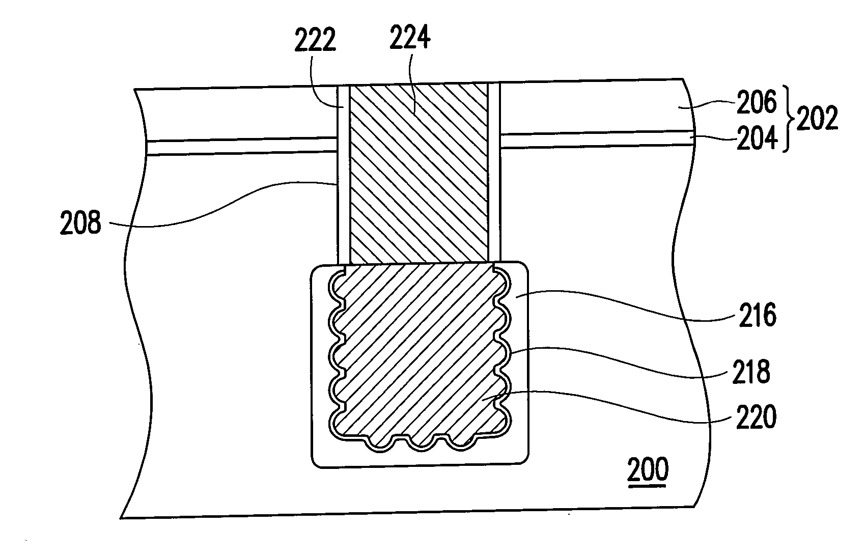
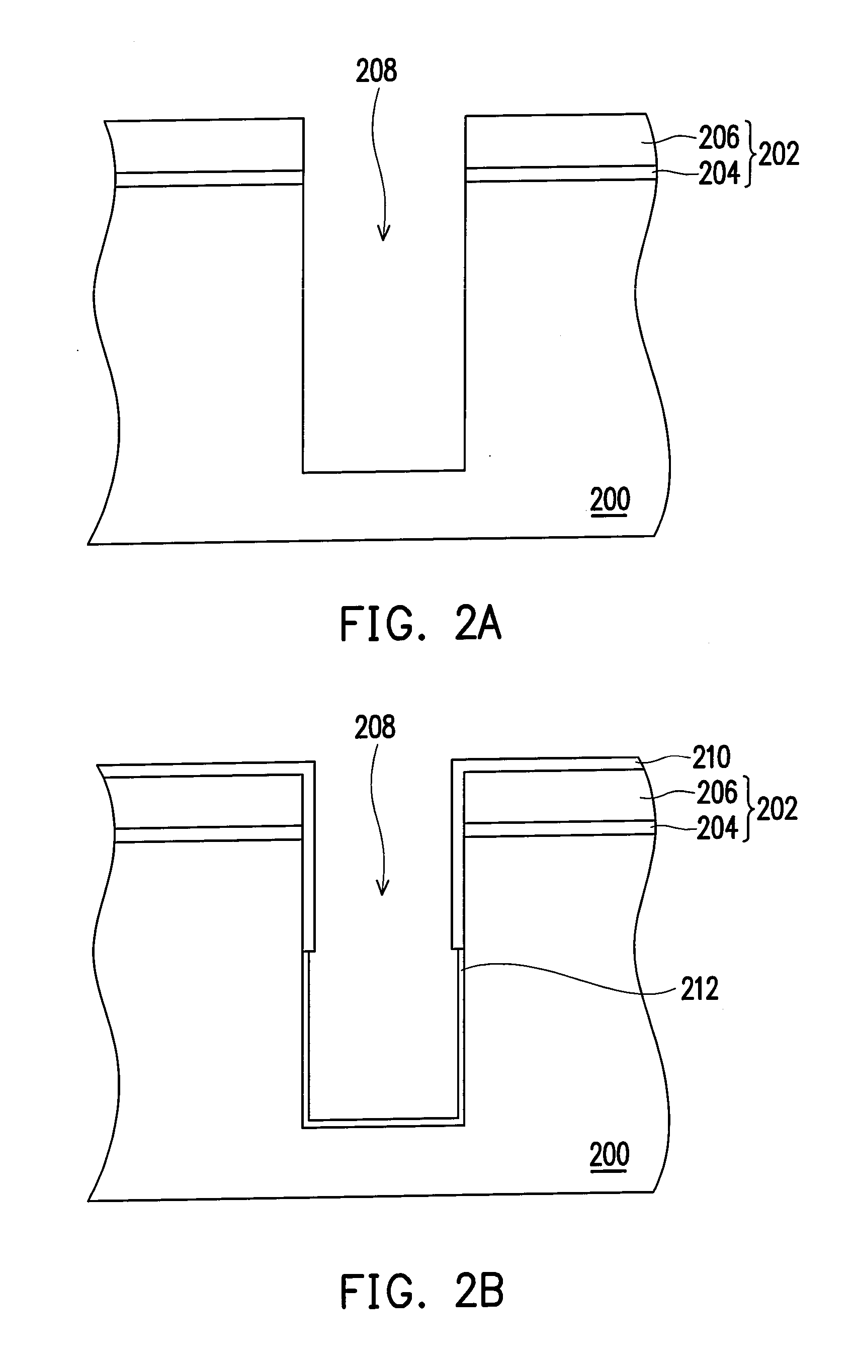
[0046]FIGS. 2A-2H are cross-sectional views illustrating the steps for fabricating a trench capacitor according to an embodiment of the present invention. Initially, referring to FIG. 2A, a substrate 200 is provided, wherein the substrate 200 is a silicon substrate or other proper semiconductor substrate, for example.

[0047]Next, a patterned mask layer 202 is formed on the substrate 200. The patterned mask layer 202 is consisted of a pad oxide layer 204 and a silicon nitride layer 206, for example. For example, a method for forming the patterned mask layer 202 is started by forming a silicon oxide layer used as the pad oxide layer 204 on the substrate 200 via a thermal oxidation process. Next, a chemical vapor deposition process is performed to form a silicon nitride layer 206 on the pad oxide layer 204. Then, a photolithographic process and an etching process are performed to form the patterned mask layer 202 on the substrate 200.

[0048]After that, the substrate 200 is etched by usin...


PUM

PropertyMeasurementUnit
sizeaaaaaaaaaa
sizesaaaaaaaaaa
sizeaaaaaaaaaa

Abstract

A method of fabricating a deep trench is provided, by which a trench is formed in the substrate initially. Then, a block layer is formed on the substrate surface of the upper portion of the trench. After that, a pad oxide layer is formed on the substrate surface of the lower portion of the trench. Next, a plurality of hemispherical silicon grains is formed on the substrate and exposes a portion of the pad oxide layer. Then, by using the hemispherical silicon grains as a mask, a portion of the pad oxide layer is removed so as to form a patterned pad oxide layer. Continually, the hemispherical silicon grains and the substrate exposed by the patterned pad oxide layer are removed. Finally, the patterned pad oxide layer is removed.

Description

CROSS-REFERENCE TO RELATED APPLICATION[0001]This application claims the priority benefit of Taiwan application serial no. 96120698, filed on Jun. 8, 2007. All disclosure of the Taiwan application is incorporated herein by reference.BACKGROUND OF THE INVENTION[0002]1. Field of the Invention[0003]The present invention relates to a fabricating method of a capacitor, and more particularly, to a fabricating method of a trench capacitor.[0004]2. Description of Related Art[0005]With continually miniaturized components, sizes of electrical components are increasingly decreased. As for memory components having capacitors, the trend of size reducing means the available space used for fabricating capacitors become smaller and smaller. Hence, how to make capacitors with sufficient capacity becomes one of the most important issues to the recent semiconductor fabrication technology.[0006]Generally, there are a lot of methods for increasing the charge storage capacity of capacitors, such as decrea...

Claims


Application Information

Patent Timeline
Patent Type & Authority Applications(United States)
IPC IPC(8): H01L21/20
CPCH01L28/84
Inventor LIN, SHIAN-JYH
Owner NAN YA TECH
Why Eureka
Try Eureka