Display device

a display device and display technology, applied in the field of display devices, can solve the problems of reducing reliability and yield, affecting display quality, and difficult to obtain a completely uniform crystallization state of polycrystalline silicon, so as to prevent display unevenness, reduce image quality, and high image quality

Inactive Publication Date: 2008-12-18
SEMICON ENERGY LAB CO LTD
View PDF17 Cites 16 Cited by
  • Summary
  • Abstract
  • Description
  • Claims
  • Application Information

AI Technical Summary

Benefits of technology

[0025]Accordingly, a display device which prevents display unevenness, decrease in image quality, and the like and has high image quality and high reliability can be provided.

Problems solved by technology

However, polycrystalline silicon is difficult to obtain a completely uniform crystallization state, and variations in characteristics of transistors to be formed are generated.
When transistors having such characteristic variations are used for a display device, defects occur such that image quality is decreased because display unevenness occurs in an obtained image and such that reliability and yield are also decreased because quality of the display device to be manufactured has variations.

Method used


Image

  • Display device
  • Display device
  • Display device

Examples


embodiment mode 1

[0046]In this embodiment modes a display device for high image quality and high reliability and a method for manufacturing the display device will be described in detail with reference to FIGS. 1A and 1B, 2A to 2C, 3A to 3C, 4A to 4C, 5A to 5C, 6A to 6D, 7A to 7C, 9A and 9B and 10A to 10C.

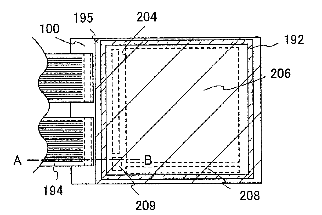
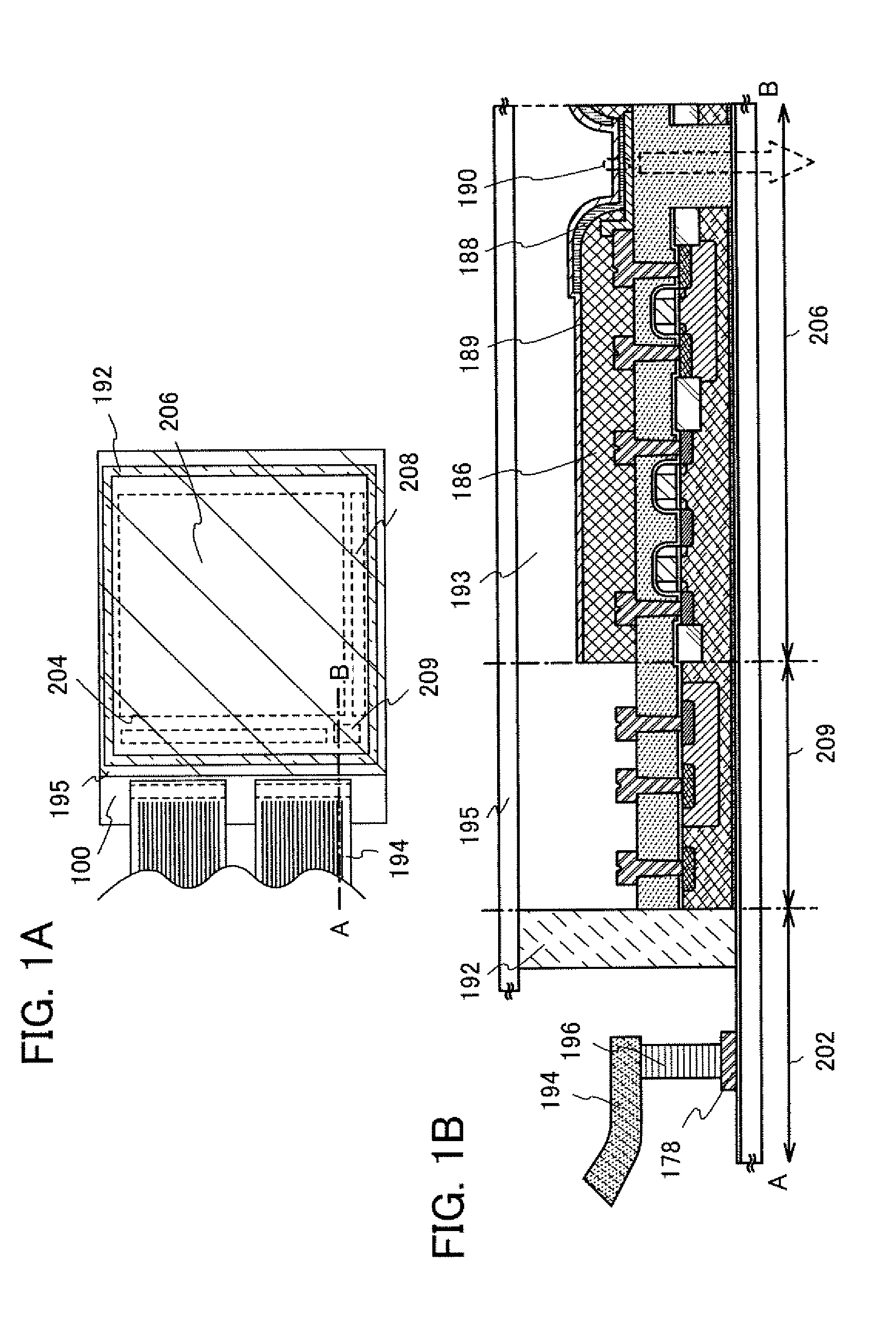
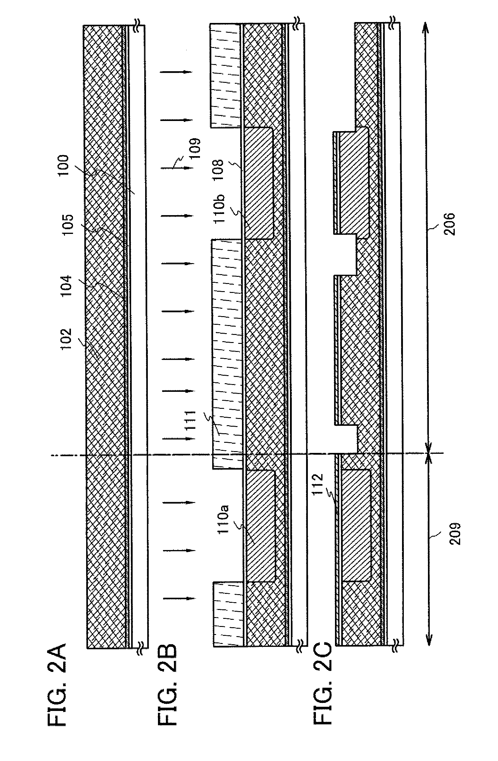
[0047]FIG. 10A is a top view illustrating a structure of a display panel of the present invention. A pixel region 2701 in which pixels 2702 are arranged in matrix, a scan line input terminal 2703, a signal line input terminal 2704, and a reference circuit 2705 are formed over a substrate 2700 having an insulating surface. The number of pixels may be decided according to various standards: if the standard is XGA, the number of pixels may be 1024×768×3 (RGB); if the standard is UXGA, the number of pixels may be 1600×1200×3 (RGB); and if the display panel is for full-spec high vision, the number of pixels may be 1920×1080×3 (RGB).

[0048]A scan line extended from the scan line input terminal 2703 and a ...

embodiment mode 2

[0145]A display device having a light-emitting element can be formed by applying the present invention. Light is emitted from the light-emitting element by any of bottom emission, top emission, and dual emission. In this embodiment mode, an example of a dual emission display device which is for achieving high reliability and has a high-quality display function with excellent visibility will be described with reference to FIG. 8.

[0146]A display device shown in FIG. 8 includes a light-transmitting element substrate 1600 having an insulating surface, a blocking layer 1601, an insulating layer 1604 having a bonding surface, a single-crystal semiconductor layer 1602, transistors 1655, 1665, 1675, and 1685, a bipolar transistor 1640, a first electrode layer 1617, an electroluminescent layer 1619, a second electrode layer 1620, a filler 1622, a sealant 1632, insulating films 1611 and 1612, an insulating layer 1614, a sealing substrate 1625, a terminal electrode layer 1681, an anisotropic c...

embodiment mode 3

[0159]This embodiment mode will describe an example of a display device for achieving high image quality and high reliability. Specifically, a light-emitting display device using a light-emitting element for a display element will be described.

[0160]In this embodiment mode, structures of light-emitting elements that can be used for display elements in the display device of the present invention will be described with reference to FIGS. 13A and 13B.

[0161]FIGS. 13A and 13B illustrate structures of a light-emitting element in which an EL layer 860 is sandwiched between a first electrode layer 870 and a second electrode layer 850. The EL layer 860 includes a first layer 804, a second layer 803, and a third layer 802 as shown in the drawings. In FIGS. 13A and 13B, the second layer 803 is a light-emitting layer, and the first layer 804 and the third layer 802 are functional layers.

[0162]The first layer 804 is a layer having a function of transporting holes to the second layer 803. In FIGS...


PUM


Abstract

A single-crystal semiconductor layer which is separated from a single-crystal semiconductor substrate, and bonded to and provided over a supporting substrate is used, whereby a transistor having uniform characteristics can be formed. A reference circuit having a bipolar transistor is provided, whereby temperature dependence of a driving transistor which is driven by supplying current to the light-emitting element of a pixel is compensated.

Description

BACKGROUND OF THE INVENTION[0001]1. Field of the Invention[0002]The present invention relates to a display device.[0003]2. Description of the Related Art[0004]Active matrix display devices in which transistors are formed over substrates as pixel switching elements have been developed, and display devices in which polycrystalline silicon is used as semiconductor layers of transistors that drive and control display elements have been put into practical use.[0005]However, polycrystalline silicon is formed in such a way that amorphous silicon is formed by a film formation method and a crystallization process is performed. Therefore, variations of a crystallization state affect characteristics of transistors which are formed. Accordingly, a crystallization condition and a crystallization method such that polycrystalline silicon with more uniform crystallized state is obtained have been researched (e.g., refer to Reference 1: Japanese Published Patent Application No. 2002-124467).[0006]In...

Claims


Application Information

Patent Timeline
Patent Type & Authority Applications(United States)
IPC IPC(8): H01L35/24H01J1/62
CPCG09G3/3233G09G3/3291G09G2300/0842G09G2320/029H01L27/1214H01L27/1266H01L27/3244H01L29/66772H10K59/12
Inventor TAKAHASHI, KEI
Owner SEMICON ENERGY LAB CO LTD
Why Eureka
Try Eureka