Partially depleted soi field effect transistor having a metallized source side halo region

a semiconductor field effect and soi technology, applied in the field of semiconductoroninsulator (soi) metal oxide semiconductor field effect transistors, can solve the problems of dynamic sub-threshold voltage (vt) leakage and threshold voltage (vt) mismatch among geometrically identical adjacent devices, and the floating body also poses leakage problems for the pass gate devi

Active Publication Date: 2008-12-18
TAIWAN SEMICON MFG CO LTD
View PDF7 Cites 46 Cited by
  • Summary
  • Abstract
  • Description
  • Claims
  • Application Information

AI Technical Summary

Benefits of technology

[0031]According to another aspect of the present invention, a semiconductor-on-insulator (SOI) m

Problems solved by technology

Furthermore, the level of leakage current also depends on the voltage of the floating body, which poses a challenge in the design of a low power SOI MOSFET.
As such, SOI MOSFETs exhibit threshold voltages which are difficult to anticipate and control, and which vary in time.
The body charge storage effects result in dynamic sub-threshold voltage (sub-Vt) leakage and threshold voltage (Vt) mismatch among geometrically identical adjacent devices.
The floating body also poses leakage problems for pass gate devices.
However, prior art methods of tying the body of a partially depleted SOI MOSFET to

Method used


Image

  • Partially depleted soi field effect transistor having a metallized source side halo region
  • Partially depleted soi field effect transistor having a metallized source side halo region
  • Partially depleted soi field effect transistor having a metallized source side halo region

Examples


Embodiment Construction

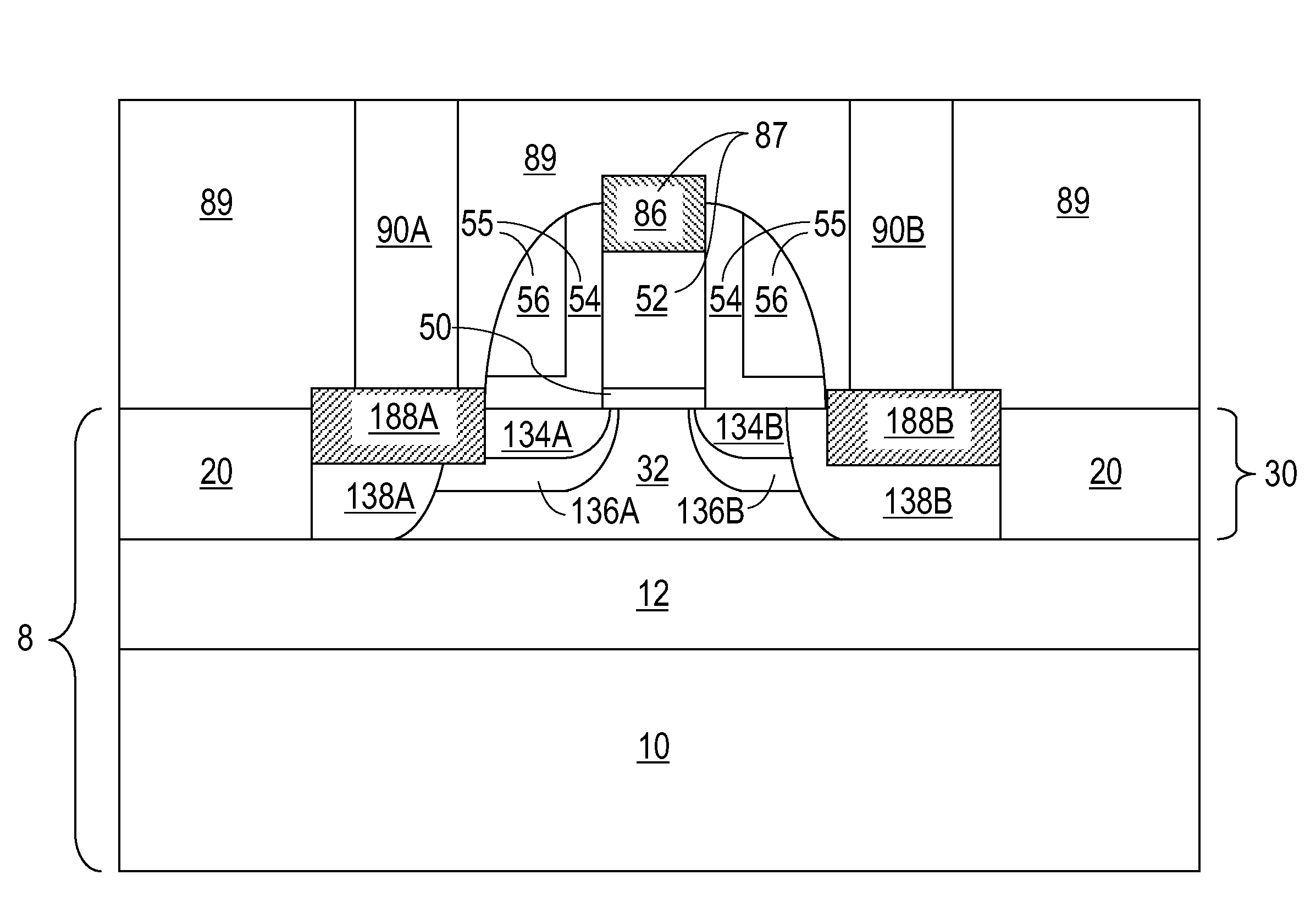
[0052]As stated above, the present invention relates to partially depleted semiconductor-on-insulator (SOI) metal oxide semiconductor field effect transistors (MOSFETs) having a metallized source side halo region and methods of manufacturing the same, which are now described in detail with accompanying figures. It is noted that like and corresponding elements are referred to by like reference numerals.

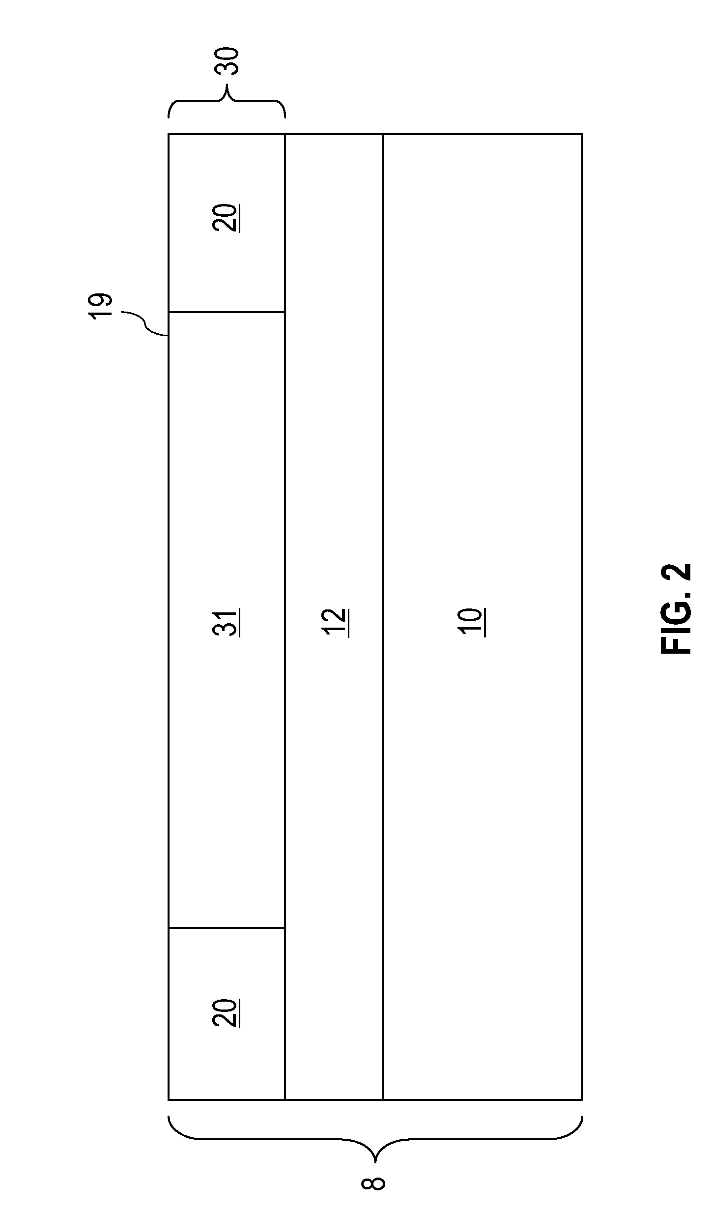
[0053]Referring to FIG. 2, an exemplary semiconductor structure comprises a semiconductor-on-insulator (SOI) metal-oxide-semiconductor field effect transistor (MOSFET) structure according to the present invention. The inventive SOI MOSFET comprises an SOI substrate 8 containing a handle substrate 10, a buried insulator layer 12, and a top semiconductor layer 30. The top semiconductor layer 30 contains shallow trench isolation 20 comprising a dielectric material and a semiconductor region 31 comprising a semiconductor material. The shallow trench isolation 20 abuts the buried insulator ...


PUM


Abstract

Source and drain extension regions and source side halo region and drain side halo region are formed in a top semiconductor layer aligned with a gate stack on an SOI substrate. A deep source region and a deep drain region are formed asymmetrically in the top semiconductor layer by an angled ion implantation. The deep source region is offset away from one of the outer edges of the at least spacer to expose the source extension region on the surface of the semiconductor substrate. A source metal semiconductor alloy is formed by reacting a metal layer with portions of the deep source region, the source extension region, and the source side halo region. The source metal semiconductor alloy abuts the remaining portion of the source side halo region, providing a body contact tied to the deep source region to the partially depleted SOI MOSFET.

Description

FIELD OF THE INVENTION[0001]The present invention relates to semiconductor devices, and particularly, to partially depleted semiconductor-on-insulator (SOI) metal oxide semiconductor field effect transistors (MOSFETs) having a metallized source side halo region and methods of manufacturing the same.BACKGROUND OF THE INVENTION[0002]On one hand, a metal oxide semiconductor field effect transistor (MOSFET) built on a silicon-on-insulator (SOI) substrate typically offers advantages over a MOSFET with comparable dimensions that is built on a bulk substrate by providing a higher on-current and lower parasitic capacitance between the body and other MOSFET components. On the other hand, a MOSFET built on an SOI substrate tends to have less consistency in the device operation due to “history effect,” or “floating body effect,” in which the potential of the body, and subsequently, the timing of the turn-on and the on-current of the SOI MOSFET are dependent on the past history of the SOI MOSFE...

Claims


Application Information

Patent Timeline
IPC IPC(8): H01L29/786H01L21/336
CPCH01L29/458H01L29/66772H01L29/78612H01L29/78624H01L29/78696
Inventor CAI, JINHAENSCH, WILFRIEDMAJUMDAR, AMLAN
Owner TAIWAN SEMICON MFG CO LTD
Why Eureka
Try Eureka