Epitaxial wafers, method for manufacturing of epitaxial wafers, method of suppressing bowing of these epitaxial wafers and semiconductor multilayer structures using these epitaxial wafers

a technology of epitaxial wafers and epitaxial layers, which is applied in the direction of polycrystalline material growth, crystal growth process, transportation and packaging, etc., can solve the problems of difficult to grow large-size bulk single-crystal gan-based compound semiconductors, disturbance of vacuum chuck properties, and inability to obtain high-quality epitaxial layers, etc., to achieve the effect of suppressing the bowing of epitaxial wafers

Active Publication Date: 2008-12-18
NGK INSULATORS LTD
View PDF5 Cites 13 Cited by
  • Summary
  • Abstract
  • Description
  • Claims
  • Application Information

AI Technical Summary

Benefits of technology

[0009]The present invention relates to a technique for suppressing the bowing of an epitaxial wafer obtained by forming a group III-nitride multilayer film on a substrate.
[0010]An epitaxial wafer according to a first aspect of the present invention comprises a substrate, at least two group III-nitride layers epitaxially formed on the substrate and at least one group III-nitride interlayer, epitaxially formed between at least two group III-nitride layers, substantially containing no Al. The growth temperature for the group III-nitride interlayer is lower than the growth temperature for each of at least two group III-nitride layers. Thus, bowing of the epitaxial wafer can be suppressed. When this epitaxial wafer is used, the chance of the vacuum chuck failing during a transfer step decreases and the exposure accuracy etc. in a photolithography step can be improved. Further, the epitaxial wafer can be prevented from cracking.
[0011]An epitaxial wafer according to a second aspect of the present invention comprises a substrate, at least two group III-nitride layers epitaxially formed on the substrate and at least one group III-nitride interlayer, epitaxially formed between at least two group III-nitride layers, substantially containing no Al, wherein the group III-nitride interlayer functions as a stress relaxation layer. When this epitaxial wafer is used, the chance of the vacuum chuck failure during a transfer step decreases and the exposure accuracy in a photolithography step can be improved. Further, the epitaxial wafer can be prevented from cracking.
[0012]An epitaxial wafer according to a third aspect of the present invention comprises a substrate, at least two group III-nitride layers epitaxially formed on the substrate and at least one group III-nitride interlayer group, epitaxially formed between at least two group III-nitride layers, substantially containing no Al and including at least one first interlayer formed at a first forming temperature and a plurality of second interlayers alternately stacked with at least one first interlayer and formed at a second growth temperature lower than the first growth temperature. The second growth temperature is also lower than the growth temperature for each of at least two group III-nitride layers. Thus, bowing of the epitaxial wafer can be suppressed. When this epitaxial wafer is used, the chance of the vacuum chuck failing during a transfer step decreases and the exposure accuracy in a photolithography step can be improved. Further, the epitaxial wafer can be prevented from cracking.
[0013]An epitaxial wafer according to a fourth aspect of the present invention comprises a substrate, at least two group III-nitride layers epitaxially formed on the substrate and at least one group III-nitride interlayer group, epitaxially formed between at least two group III-nitride layers, substantially containing no Al and including at least one first interlayer and a plurality of second interlayers formed at a growth temperature different from that of the first interlayer and alternately stacked with at least one first interlayer, wherein the group III-nitride interlayer group functions as a stress relaxation layer. Thus, bowing of the epitaxial wafer can be suppressed. When this epitaxial wafer is used, the chance of the vacuum chuck failing during a transfer step decreases and the exposure accuracy in a photolithography step can be improved. Further, the epitaxial wafer can be prevented from cracking.

Problems solved by technology

It is difficult to grow large-size bulk single-crystal GaN-based compound semiconductors.
However, a mismatch of the lattice constants between the GaN-based compound semiconductor and the substrates is so large that a high-quality epitaxial layer can not be obtained by directly forming the target GaN-based compound semiconductor on the substrate.
This bowing disturbs the vacuum chuck properties during transfer steps or reduces the exposure accuracy in a photolithography step.
Further, this bowing may cause cracking on the epitaxial wafer.

Method used


Image

  • Epitaxial wafers, method for manufacturing of epitaxial wafers, method of suppressing bowing of these epitaxial wafers and semiconductor multilayer structures using these epitaxial wafers
  • Epitaxial wafers, method for manufacturing of epitaxial wafers, method of suppressing bowing of these epitaxial wafers and semiconductor multilayer structures using these epitaxial wafers
  • Epitaxial wafers, method for manufacturing of epitaxial wafers, method of suppressing bowing of these epitaxial wafers and semiconductor multilayer structures using these epitaxial wafers

Examples


example 1

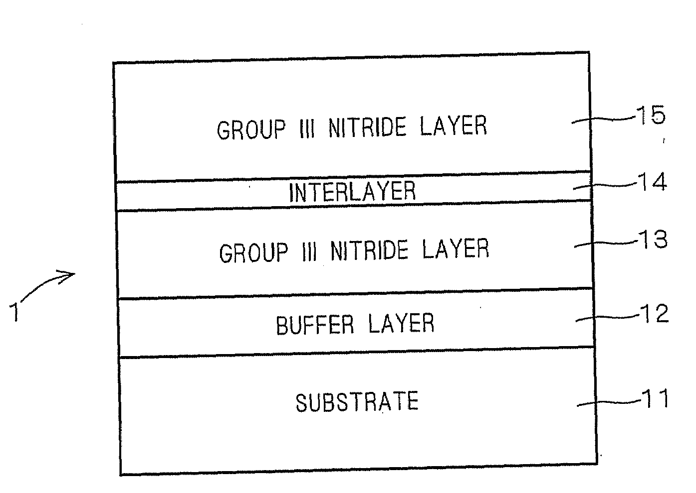
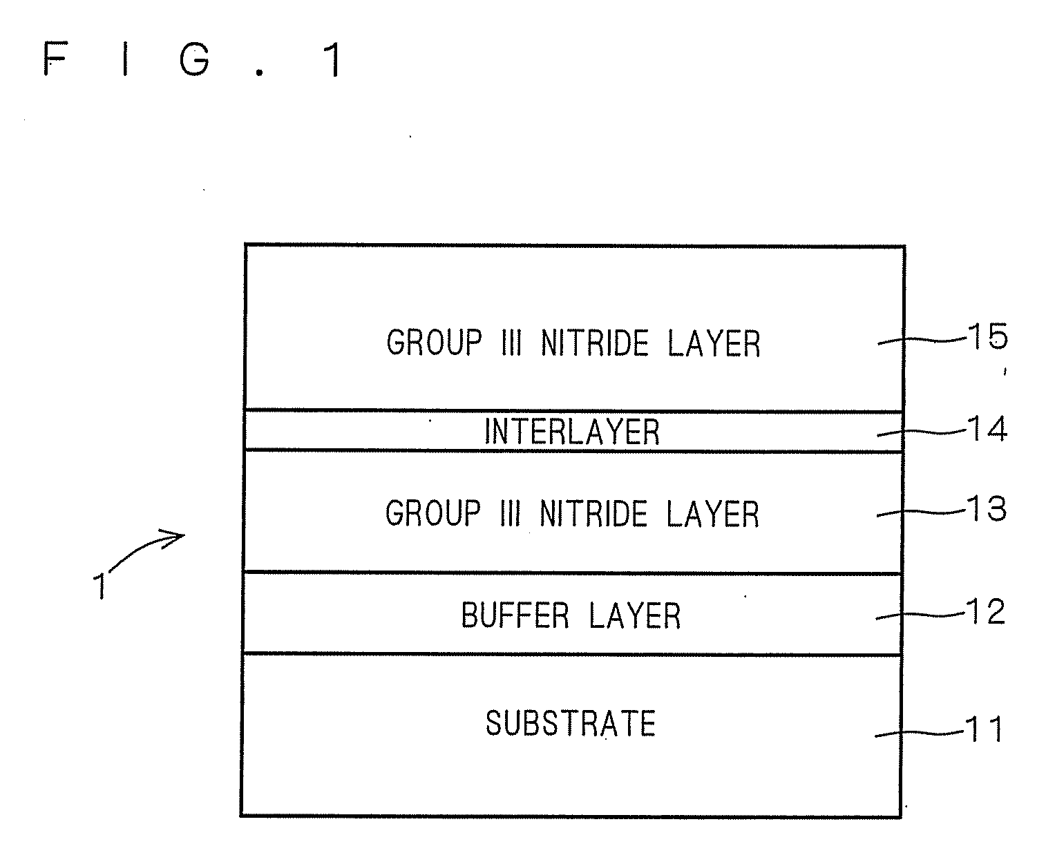
[0045]A method for manufacturing an epitaxial wafer 100 including a GaN interlayer, which is grown at 500° C. and does not substantially contain Al according to Example 1 is described with reference to the process flow chart shown in FIG. 3, and a method for forming a semiconductor multilayer structure on this epitaxial wafer 100 is described with reference to the process flow chart shown in FIG. 4. The process flow charts shown in FIGS. 3 and 4 are model diagrams conceptually illustrating the states of the epitaxial wafer 100 in respective steps, and hence, the thicknesses of layers illustrated in these figures do not necessarily reflect the thickness ratios in the practical epitaxial wafer 100. This also applies to subsequent process flow charts.

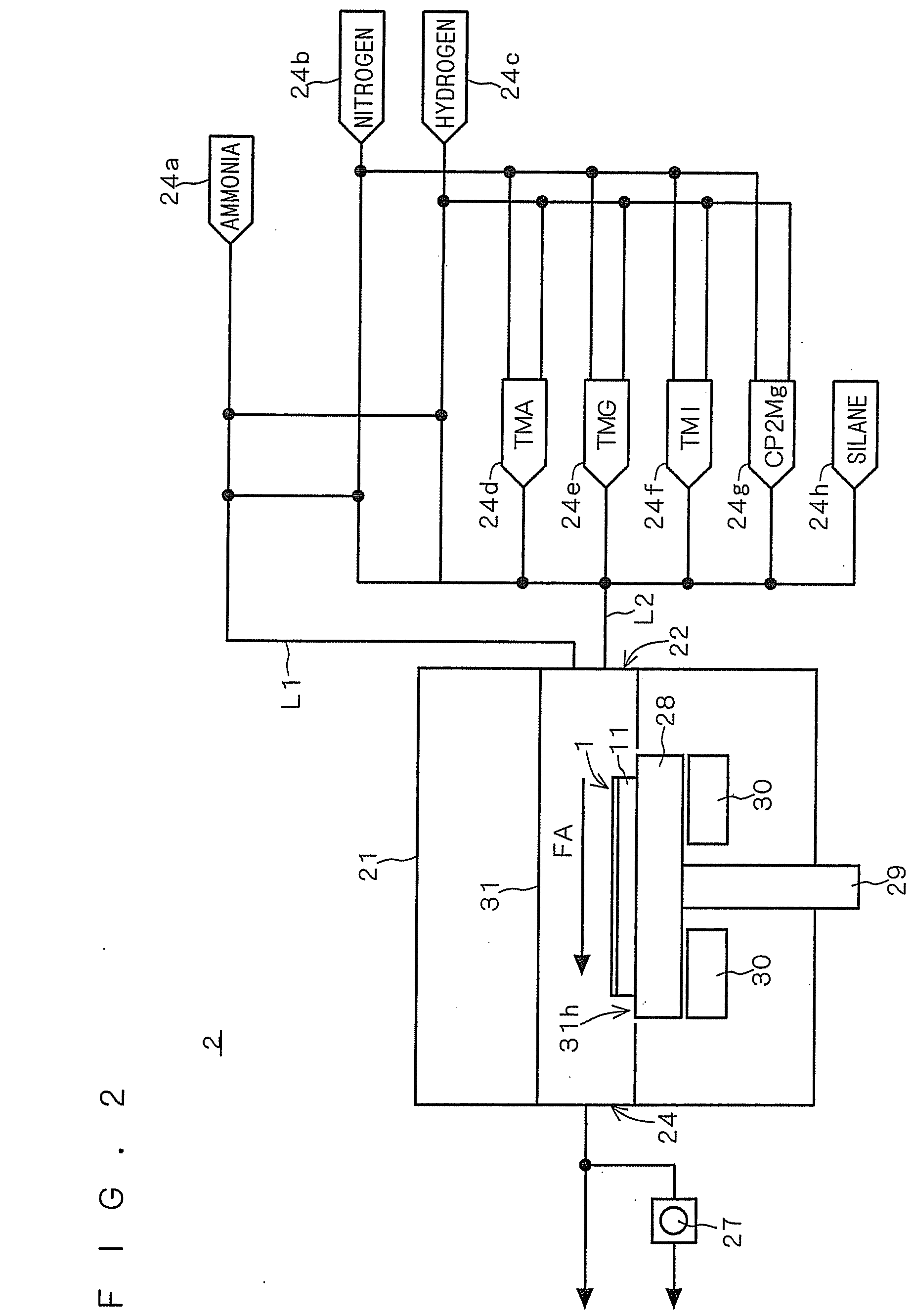
[0046]According to Example 1, a substantially circular C-plane single-crystal two-inch-diameter 330-μm-thick sapphire substrate was employed as a substrate 111. In advance of formation of epitaxial layers on the main surface of the substra...

examples 2 to 5

[0058]Epitaxial wafers according to Examples 2, 3 and 4 correspond to those obtained by changing the thicknesses of GaN interlayers similar to that of the epitaxial wafer 100 according to Example 1 from 20 nm to 5 nm, 50 nm and 100 nm, respectively. The epitaxial wafer according to Example 5 was obtained by changing the epitaxial formation temperature of a GaN interlayer similar to that of the epitaxial wafer 100 according to Example 1 from 500° C. to 800° C.

[0059]FIG. 9 shows the dependence of the bowing value BW on the thicknesses of the GaN interlayers for the respective types (GaN and AlN) of interlayers according to Examples 1 to 4 and Comparative Example 1 having interlayers that are grown at a temperature of 500° C., and a sample according to Comparative Example 2 without an interlayer. FIG. 10 shows the dependence of the bowing values BW on the growth temperatures for the GaN interlayers of Examples 1 to 5 with GaN interlayers having a thickness of 20 nm and the sample accor...

example 6

[0060]While a single GaN interlayer was formed as a stress relaxation layer in each of Examples 1 to 5, the stress relaxation layer may alternatively be formed by an interlayer group including a plurality of layers. A method for manufacturing of an epitaxial wafer 400 having an interlayer group including a plurality of layers according to Example 6 is described with reference to the process flow chart shown in FIG. 11, and a method of forming a semiconductor multilayer structure on this epitaxial wafer 400 is described with reference to the process flow chart shown in FIG. 12.

[0061]A low-temperature-deposited buffer layer 412 of GaN having a thickness of 30 nm and a GaN layer 413 having a thickness of 0.5 μm were epitaxially formed on a base 411 similar to that used in Example 1 under the same conditions as those in Example 1 ([b] and [c] in FIG. 11). Then, a GaN interlayer group 414 was epitaxially formed on the GaN layer 413 ([d] in FIG. 11). The GaN interlayer group 414 was prepa...


PUM

PropertyMeasurementUnit
thicknessaaaaaaaaaa
thicknessaaaaaaaaaa
temperatureaaaaaaaaaa

Abstract

A technique for suppressing the bowing of an epitaxial wafer is provided. The epitaxial wafer is prepared by successively epitaxially growing a target group III-nitride layer, an interlayer and another group III-nitride layer on a substrate with a buffer layer. The interlayer is mainly composed of a mixed crystal of GaN and InN expressed in a general formula (GaxIny)N (0≦x≦1, 0≦y≦1, x+y=1) (or a crystal of GaN), and does not contain Al. The interlayer is epitaxially formed at a lower growth temperature than those of the group III-nitride layers, more specifically at a temperature in a range of at least 350° C. to not more than 1000° C.

Description

CROSS REFERENCE TO RELATED APPLICATIONS[0001]This application is a continuation of U.S. patent application Ser. No. 10 / 909,477, filed Aug. 2, 2004, which claims the benefit of Japanese Application No. 2003-205728, filed Aug. 4, 2003, and Japanese Application No. 2004-178644, filed Jun. 16, 2004, the entireties of which are incorporated herein by reference.BACKGROUND OF THE INVENTION[0002]1. Field of the Invention[0003]The present invention relates to a technique for suppressing the bowing of an epitaxial wafer prepared by forming a group III-nitride multilayer film on a substrate.[0004]2. Description of the Background Art[0005]Group III-nitride semiconductors such as GaN-based compound semiconductors have a wide band gap, a high breakdown voltage and high saturation electron velocity compared with other semiconductors. Therefore, the group III-nitride semiconductors have frequently been studied as the material for optical devices such as light-emitting diodes, laser diodes (LDs) and...

Claims


Application Information

Patent Timeline
Patent Type & Authority Applications(United States)
IPC IPC(8): H01L29/20B32B7/00H01L21/20C30B25/20C30B29/40H01L21/205H01L33/12H01L33/32
CPCC30B25/20C30B29/403H01L21/0237H01L21/0242H01L21/02458Y10T428/24942H01L21/0254H01L21/02576H01L21/02579H01L21/0262H01L21/02661H01L21/02505
Inventor SAKAI, MASAHIROTANAKA, MITSUHIROEGAWA, TAKASHI
Owner NGK INSULATORS LTD
Why Eureka
Try Eureka