Plasma etching method for etching an object

a technology of etching method and object, which is applied in the direction of basic electric elements, semiconductor/solid-state device manufacturing, electric apparatus, etc., can solve the problems of deteriorating the etching rate at the high aspect ratio portion, unable to exert etching resistance and shrinking effect of the mask, and difficulty in deposited a sufficient amount of amorphous carbon film, etc., to achieve high industrial applicability and improve yield

Inactive Publication Date: 2010-11-25
HITACHI HIGH-TECH CORP
View PDF52 Cites 26 Cited by
  • Summary
  • Abstract
  • Description
  • Claims
  • Application Information

AI Technical Summary

Benefits of technology

[0009]The etching method disclosed in patent document 2 solves the tradeoff relationship between the mask selective ratio and etch stop, but it does not suppress bowing occurring during etching of a low or middle aspect ratio portion performed from the initial to the middle stages of etching by controlling the shape of the leading end portion of the mask. Further, the method focuses on the fact that etch stop does not occur easily while etching a high aspect ratio portion, and improves the mask selective ratio by increasing the deposition rate at the last stage of etching, but this method may further deteriorate the lowering of etching rate at the high aspect ratio portion.
[0010]The present invention aims at solving the problems of the prior art by providing a plasma etching method for etching an object so as to perform deep hole processing with a high aspect ratio using a plasma etching apparatus, capable of suppressing bowing occurring at the side wall of the opening of the object to be etched and solving the lack of opening at the bottom portion of the high aspect ratio portion.
[0011]The present invention aims at providing a plasma etching method for subjecting an object to be etched to ultrafine processing with a high aspect ratio, wherein during etching of a low or middle aspect ratio portion at the former half of the process for etching an object, deposits are attached to the side wall of the opening close to the surface of the mask while performing etching, and at the same time, a high mask selective ratio is realized, so as to prevent the occurrence of bowing of the object to be etched. Further according to the present invention, during etching of a high aspect ratio portion at the latter half the etching process, the deposits deposited on the side wall of the opening close to the mask surface is removed, and at the same time, ions having high directionality are entered so as to reduce the incident ions on the side wall causing bowing, thereby providing a plasma etching method capable of ensuring the bottom CD without causing increase of bowing of the object to be etched and deterioration of etch rate.
[0012]In order to solve the above-described problems, the present invention provides a plasma etching method for etching an object to be etched in a plasma etching apparatus using a mask having been patterned and formed on the object to be etched, comprising a first step for increasing the deposition rate and attaching deposits on the side wall of the opening close to the surface of the mask so as to narrow the opening, and a second step performed subsequently after the first step for reducing the deposition rate compared to the first step and etching the deposits deposited on the side wall of the opening close to the surface of the mask, according to which the deposits deposited on the side wall of the opening close to the surface of the mask for narrowing the opening in the first step are etched in the second step so as to reduce (remove) the deposits and to improve the directionality of ions being incident on the object to be etched.
[0023]According to the plasma etching method of the present invention, a scatterometry is adopted for detecting an etching profile and performing feedback control, so as to control the etching profile stably for a long period of time.
[0025]The plasma etching method according to the present invention has high industrial applicability, since it enables to improve the yield in the process of manufacturing semiconductors.

Problems solved by technology

According to this method, during the process of forming fine holes, there is fear that the deposition of the amorphous carbon film may close the opening of the mask pattern, so it was difficult to deposit a sufficient amount of amorphous carbon film.
Further according to the method, when deep hole processing having a high aspect ratio is performed in a state where the amount of deposition of the amorphous carbon film is insufficient, the amorphous carbon film is removed via sputtering or the like at the initial stage of the etching process, and at the latter half of the etching process, sufficient etching resistance and shrinking effect of the mask may not be exerted.
The etching method disclosed in patent document 2 solves the tradeoff relationship between the mask selective ratio and etch stop, but it does not suppress bowing occurring during etching of a low or middle aspect ratio portion performed from the initial to the middle stages of etching by controlling the shape of the leading end portion of the mask.
Further, the method focuses on the fact that etch stop does not occur easily while etching a high aspect ratio portion, and improves the mask selective ratio by increasing the deposition rate at the last stage of etching, but this method may further deteriorate the lowering of etching rate at the high aspect ratio portion.

Method used


Image

  • Plasma etching method for etching an object
  • Plasma etching method for etching an object
  • Plasma etching method for etching an object

Examples


embodiment 1

[0047]In the present embodiment, a plasma etching method for etching an object using a patterned mask formed on the object to be etched will be described, comprising a first step of depositing deposits on a side wall of an opening close to an opening on the surface of the patterned mask during etching of the object to thereby narrow the opening and confine the occurrence of bowing to the side wall of the opening of the mask below the mask surface, and a second step of etching the object to be etched while etching the deposits deposited on the side wall of the opening close to the surface of the mask, thereby suppressing bowing of the side wall of the opening of the object to be etched.

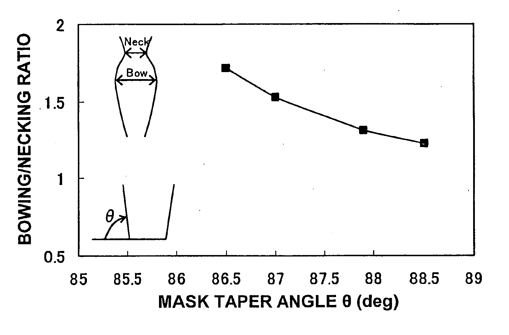
[0048]In the process of etching deep holes (high aspect ratio holes), when etching is performed under a condition in which the mask selective ratio (etching rate of object to be etched / etching rate of mask) is low, the leading end portion of the opening formed on the surface of the mask is gradually re...

embodiment 2

[0061]The present embodiment illustrates an etching method comprising sequentially performing a first step for etching an object to be etched by narrowing the opening close to the surface of the mask pattern by deposits, and a second step for etching the object to be etched while removing the deposits on the opening close to the surface of the mask pattern, thereby suppressing the shrinkage of processing dimension at the bottom portion of the hole and solving the deterioration of etch rate in a high aspect ratio.

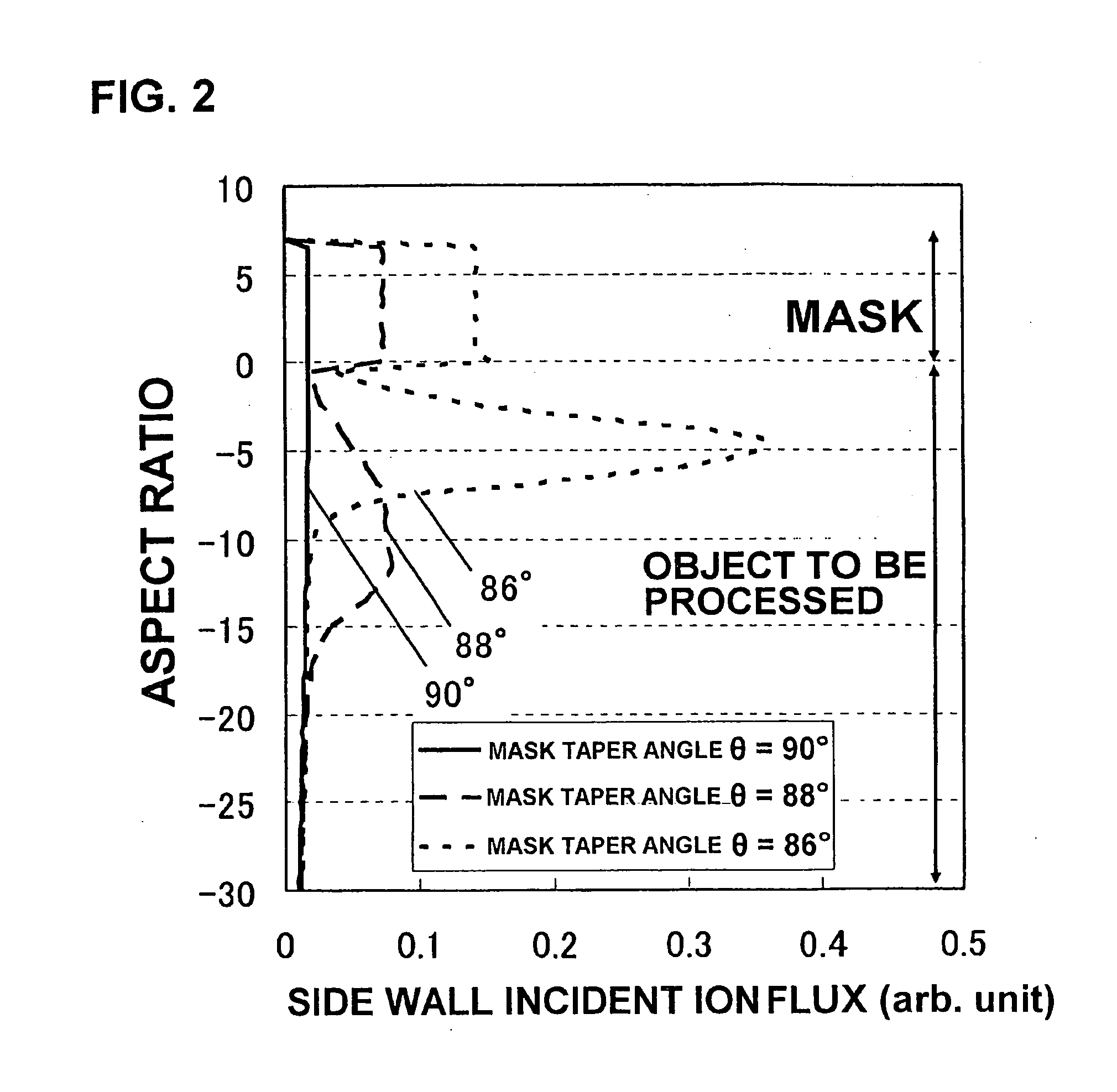
[0062]Embodiment 1 illustrates a method for suppressing the occurrence of bowing in the object to be etched by narrowing the opening close to the surface of the mask. However, by narrowing the opening close to the surface of the mask, the efficient mask diameter is reduced, and the processing dimension of the bottom portion of the hole (bottom CD) may fall below the design value. Further, the incident ions have a certain dispersion angle by the collision with neutral gas or ...

embodiment 3

[0072]An etching method for controlling the etching profile stably for a long period of time with respect to the method for etching an object to be etched illustrated in embodiments 1 and 2 will now be described.

[0073]At first, the outline of the structure of a plasma etching apparatus for performing the plasma etching method according to the present invention will be illustrated in FIG. 10. The embodiment of FIG. 10 illustrates a basic structure of the plasma etching apparatus for realizing the present invention. The plasma etching apparatus comprises magnetic field coils 107 disposed on a vacuum reactor 101 having a gas introducing means 108 and an evacuation means 117, wherein the mutual reaction between the electromagnetic waves supplied through coaxial cables to the antenna 109 and the magnetic field generated by the magnetic field coils 107, the gas introduced to the vacuum reactor 101 is turned into plasma. At this time, by applying electromagnetic waves provided from a bias ...


PUM


Abstract

The invention provides a plasma etching method capable of suppressing bowing of an opening of the object to be etched, and solving the lack of opening at a high aspect ratio portion in deep hole processing having a high aspect ratio. A plasma etching method for etching an object to be etched in a plasma etching apparatus using a mask patterned and formed on the object to be etched comprises sequentially performing a first step for etching the mask while attaching deposits on a side wall of an opening close to a surface of the mask pattern of the mask using fluorocarbon gas CxFy (x=1, 2, 3, 4, 5, 6, y=4, 5, 6, 8), and a second step for etching the object to be etched while removing the deposits attached to the side wall of the opening close to the surface of the mask pattern of the mask using fluorocarbon gas.

Description

[0001]The present application is based on and claims priority of Japanese patent application No. 2009-124508 filed on May 22, 2009, the entire contents of which are hereby incorporated by reference.BACKGROUND OF THE INVENTION[0002]1. Field of the Invention[0003]The present invention relates to a plasma etching method for etching an object using a plasma etching apparatus for manufacturing semiconductors.[0004]2. Description of the Related Art[0005]In the art of forming memories such as DRAMs, there are demands to perform ultrafine hole processing having an aspect ratio of 30 or greater with a hole diameter of 70 nm or smaller, so as to secure a sufficient electrostatic capacity in a small area. Further, the pitch of patterns have become narrower so as to ensure high level integration and minimum capacity, and therefore, it has become an important issue to suppress the occurrence of bowing and to improve the mask selective ratio when etching the object to be etched. Furthermore, impo...

Claims


Application Information

Patent Timeline
Patent Type & Authority Applications(United States)
IPC IPC(8): H01L21/3065
CPCH01L21/31144H01L21/31116H01L21/3065H10B99/00
Inventor MIYAKE, MASATOSHINEGISHI, NOBUYUKIOYAMA, MASATOSHIKANEKIYO, TADAMITSUIZAWA, MASARU
Owner HITACHI HIGH-TECH CORP
Why Eureka
Try Eureka