Fabrication of semiconductor architecture having field-effect transistors especially suitable for analog applications

a field-effect transistor and semiconductor technology, applied in the field of semiconductor architecture, can solve the problems of many requirements imposed on analog igfet performance that conflict with the results of digital scaling, the operation of the igfet cannot be controlled with the gate electrode, and the weakened analog performance, etc., to achieve excellent analog performance and low parasitic capacitance

Active Publication Date: 2008-12-18
NAT SEMICON CORP
View PDF14 Cites 64 Cited by
  • Summary
  • Abstract
  • Description
  • Claims
  • Application Information

AI Technical Summary

Benefits of technology

[0026]The present invention furnishes a process for fabricating such an architecture. More particularly, a semiconductor structure fabricated according to the invention contains a principal IGFET having comparatively low parasitic capacitance along at least one of the pn junctions that form source / drain boundaries. Although usable in digital applications, the principal IGFET is particularly suitable for analog applications and can achieve excellent analog performance.

Problems solved by technology

When punchthrough occurs, the operation of the IGFET cannot be controlled with its gate electrode.
Although it would be economically attractive to utilize the same transistors for the analog and digital blocks, doing so would typically lead to weakened analog performance.
Many requirements imposed on analog IGFET performance conflict with the results of digital scaling.
Hence, linearity demands on analog transistors are very high.
Because the resultant dimensional spreads are inherently large, parameter matching in digital circuitry is often relatively poor.

Method used


Image

  • Fabrication of semiconductor architecture having field-effect transistors especially suitable for analog applications
  • Fabrication of semiconductor architecture having field-effect transistors especially suitable for analog applications
  • Fabrication of semiconductor architecture having field-effect transistors especially suitable for analog applications

Examples


Embodiment Construction

Reference Notation and Other Conventions

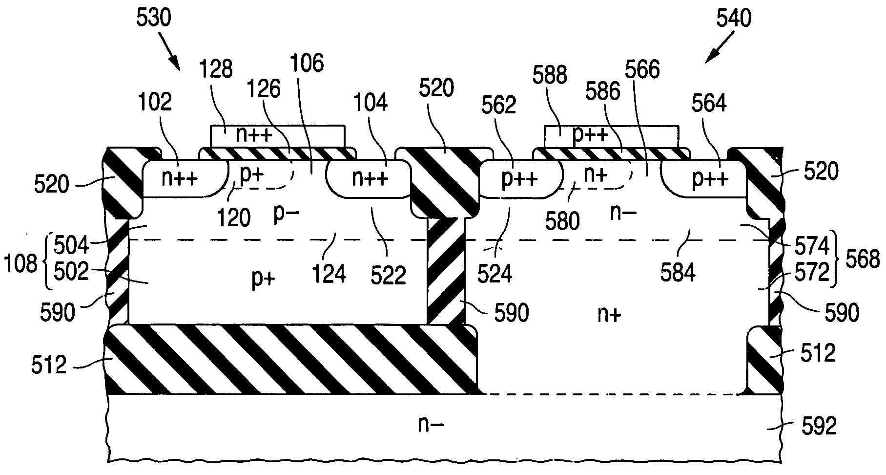
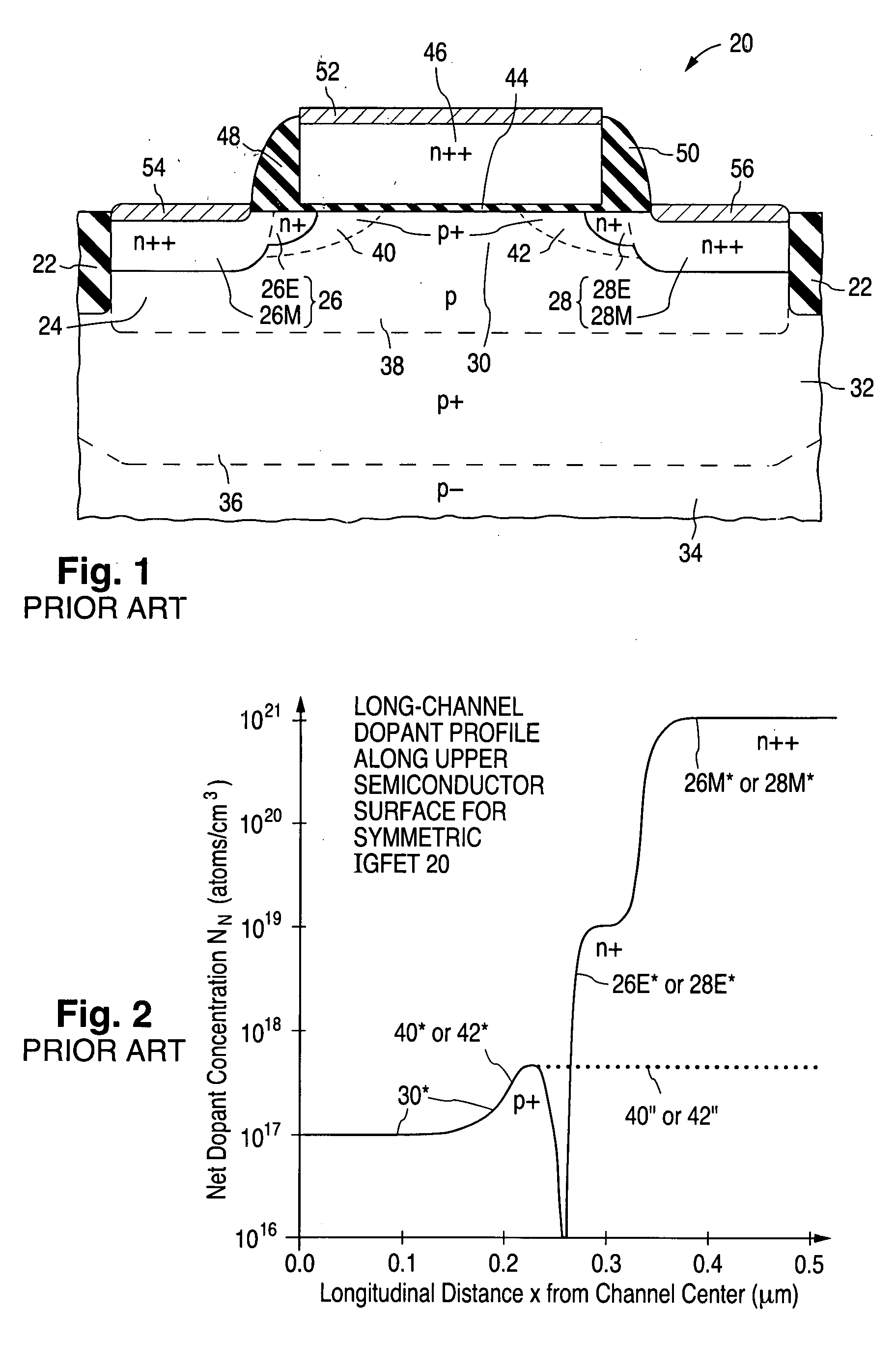
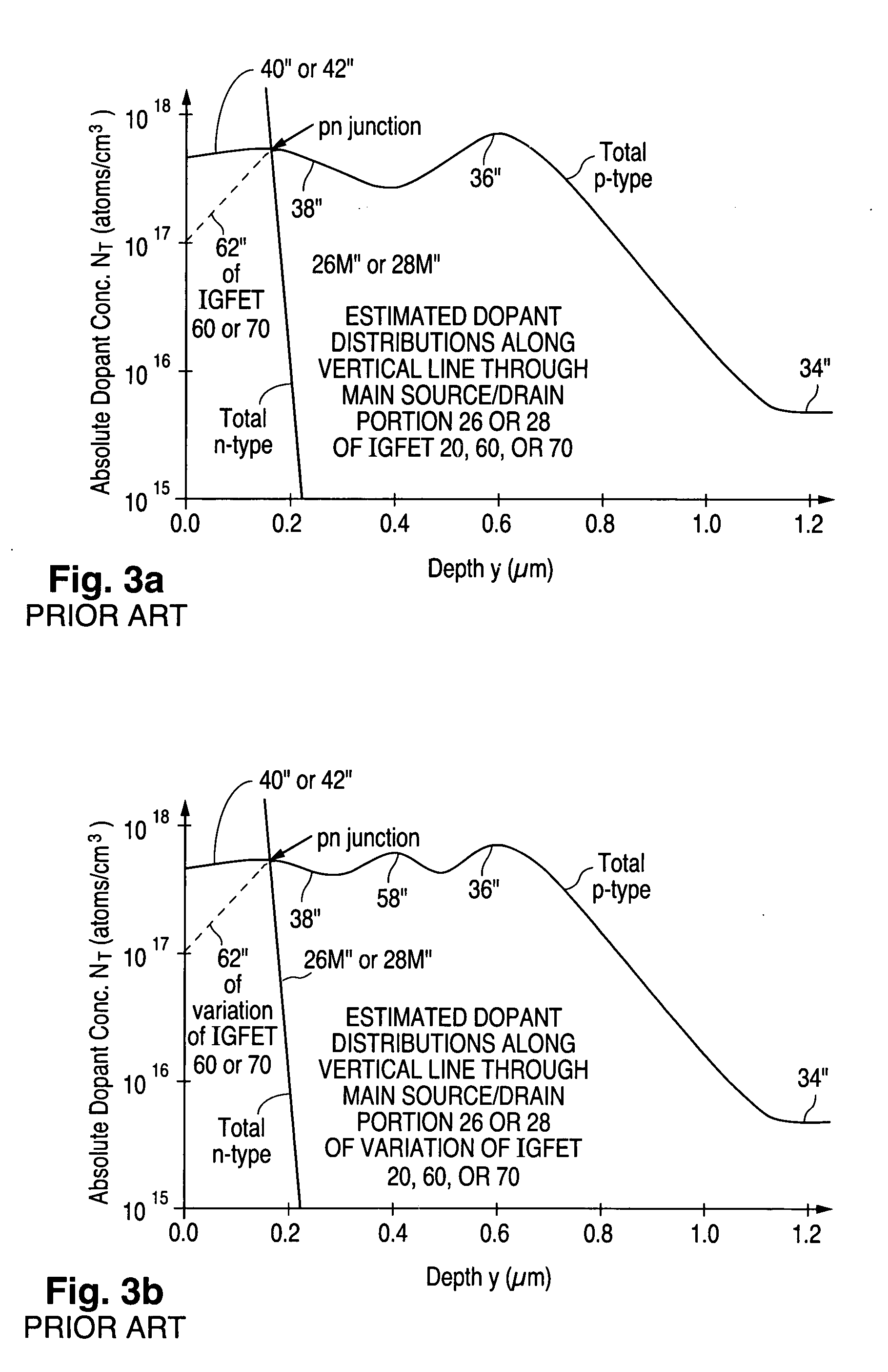
[0109]The reference symbols employed below and in the drawings have the following meanings where the adjective “lineal” means per unit IGFET width and where the adjective “areal” means per unit lateral area:[0110]AI≡current gain[0111]Cda≡areal depletion-region capacitance[0112]Cd0a≡value of areal depletion-region capacitance at zero reverse voltage[0113]CDB≡drain-to-body capacitance[0114]CDBw≡lineal drain-to-body capacitance[0115]CGB≡gate-to-body capacitance[0116]CGD≡gate-to-drain capacitance[0117]CGIa≡areal gate dielectric capacitance[0118]CGS≡gate-to-source capacitance[0119]CL≡load capacitance[0120]CSB≡source-to-body capacitance[0121]CSBw≡lineal source-to-body capacitance[0122]f≡frequency[0123]fT≡cut-off frequency[0124]fTpeak≡peak value of cut-off frequency[0125]gm≡intrinsic transconductance of IGFET[0126]gmw≡lineal transconductance of IGFET[0127]gmb≡transconductance of body electrode[0128]gmeff≡effective transconductance of IGFET in presenc...


PUM


Abstract

An insulated-gate field-effect transistor (100, 100V, 140, 150, 150V, 160, 170, 170V, 180, 180V, 190, 210, 210W, 220, 220U, 220V, 220W, 380, or 480) is fabricated so as to have a hypoabrupt vertical dopant profile below one (104 or 264) of its source/drain zones for reducing the parasitic capacitance along the pn junction between that source/drain zone and adjoining body material (108 or 268). In particular, the concentration of semiconductor dopant which defines the conductivity type of the body material increases by at least a factor of 10 in moving from that source/drain zone down to an underlying body-material location no more than 10 times deeper below the upper semiconductor surface than that source/drain zone. The body material is preferably provided with a more heavily doped pocket portion (120 or 280) situated along the other source/drain zone (102 or 262). The combination of the hypoabrupt vertical dopant profile below the first-mentioned source/drain zone, normally serving as the drain, and the pocket portion along the second-mentioned source/drain zone, normally serving as the source, enables the resultant asymmetric transistor to be especially suitable for high-speed analog applications.

Description

CROSS-REFERENCE TO RELATED APPLICATIONS[0001]This is a continuation-in-part of U.S. patent application Ser. No. 11 / 215,537, filed 29 Aug. 2005. This is also related to co-filed U.S. patent application ______, attorney docket no. NS-6271-3P US. All of the material in U.S. application Ser. Nos. 11 / 215,537 and ______, attorney docket no. NS-6271-3P US, is incorporated by reference herein to the extent not expressly repeated herein.FIELD OF USE[0002]This invention relates to semiconductor technology and, in particular, to field-effect transistors (“FETs”) of the insulated-gate type. All of the insulated-gate FETs (“IGFETs”) described below are surface-channel enhancement-mode IGFETs except as otherwise indicated.BACKGROUND[0003]An IGFET is a semiconductor device in which a gate dielectric layer electrically insulates a gate electrode from a channel zone extending between a source zone and a drain zone. The channel zone in an enhancement-mode IGFET is part of a body region, often termed ...

Claims


Application Information

Patent Timeline
Patent Type & Authority Applications(United States)
IPC IPC(8): H01L21/336
CPCH01L21/823807H01L21/823878H01L21/823892H01L27/1203H01L29/1045H01L29/7835H01L29/66659H01L29/665
Inventor BULUCEA, CONSTANTIN
Owner NAT SEMICON CORP
Why Eureka
Try Eureka