Liquid crystal display device and method of fabricating the same

a liquid crystal display and display device technology, applied in non-linear optics, instruments, optics, etc., can solve the problems of inability to control the refractive index, the region where the tfts can be driven stably the region where the tfts can be driven from the desired region, etc., to achieve uniform alignment of liquid crystal molecules and stable operation

Inactive Publication Date: 2008-12-25
SHARP KK
View PDF37 Cites 20 Cited by
  • Summary
  • Abstract
  • Description
  • Claims
  • Application Information

AI Technical Summary

Benefits of technology

[0027]The present invention aims to solve the above-enumerated problems of the prior art and to provide a method of fabricating a liquid crystal display device which, during fabrication of the liquid crystal display device, controls the alignment of liquid crystal molecules when radiating light onto a liquid crystal composition containing a photosensitive material, and thereby achieves substantially uniform alignment of the liquid crystal molecules and ensures stable operation. The invention also aims to provide such a liquid crystal display device.

Problems solved by technology

If the initial alignment is not stable, when a voltage is applied to the liquid crystal, the liquid crystal molecules do not align in a predictable manner, resulting in an inability to control the refractive index.
However, when such a liquid crystal exposure method is employed, if there is a line defect due to a bus line break or short, as shown in FIG. 3, the liquid crystal will be exposed to light when the liquid crystal in the affected area cannot be driven, and a pretilt angle different from that in other areas will be formed in this defect area, resulting in the problem that the brightness in this area differs from the brightness in other areas.
Or, in the TFT channel ON state, a shift in the TFT threshold value can occur due to exposure to ultraviolet radiation, as shown in FIG. 4, resulting in the problem that the region where the TFTs can be driven stably shifts from the desired region.
In the IPS mode, liquid crystal molecules are switched in the horizontal plane by using comb-shaped electrodes, but a strong backlight is required because the comb-shaped electrodes significantly reduce the numerical aperture.
The decrease in the effective numerical aperture due to the protrusions or slits used in MVA is not so large as that caused by the comb-electrodes in IPS, but compared with TN mode displays, the light transmittance of the liquid crystal panel is low, and it has not been possible to employ MVA for notebook computers that require low power consumption.
Furthermore, areas where the tilt direction of the liquid crystal molecules is displaced from the predefined direction inevitably exist because of the effects of the horizontal electric field, etc. at the time of driving or irregularities in the structure.
With this technique, however, if the polymerization is insufficient, image sticking can occur.
This is believed to occur because the rigidity of the polymerized polymer is insufficient and deformation occurs due to the realignment of the liquid crystal molecules at the time of voltage application.
On the other hand, to sufficiently polymerize the polymer, the duration of light radiation must be increased, but in that case, take time at the time of volume production becomes a problem.
To obtain sufficient transmittance, it is preferable to reduce the area occupied by the alignment control members by forming them spaced farther apart, but this would in turn slow the propagation speed of the tilt, resulting in a slow response speed.
However, in the case of a liquid crystal display device in which the tilt direction of the liquid crystal molecules is defined by polymerizing the polymerizable component in the liquid crystal while applying a voltage, there arises the problem that display unevenness occurs after the polymerization of the polymerizable component, because of the separation of the liquid crystal and the polymerizable component which occurs when the liquid crystal material is injected at high speed at the initial stage of injection or when there is an abrupt change in speed near a frame edge.
Fabrication of such a liquid crystal display device therefore has involved the problem that the number of processing steps increases.
Furthermore, forming the protrusions within display pixels leads to the problem that the numerical aperture decreases, reducing the transmittance.
However, if the polymer composition that defines the alignment direction does not have a sufficient cross-linked structure, the polymer becomes flexible, and its restoring force weakens.
This means that the voltage-transmittance characteristic has changed, and this defect manifests itself as a pattern image sticking.
In connection with a sixth aspect of the invention, in an MVA-LCD in which liquid crystals having a negative dielectric anisotropy are vertically aligned, and in which the alignment of the liquid crystal in the presence of an applied voltage is controlled in a number of predefined directions, without using a rubbing treatment but by utilizing the banks or slits formed on the substrates, the LCD provides excellent viewing angle characteristics compared with conventional TN mode LCDs, but there is a disadvantage that white brightness is low and the display is therefore relatively dark.
To improve this, the spacing between the banks or slits should be made sufficiently wide, but in that case, as the number of banks or slits for controlling the liquid crystal alignment decreases, it takes time until the alignment stabilizes, thus slowing the response speed.
It has, however, been found that this method has a number of problems associated with display unevenness.
That is, as this method is a rubbing-less method, if there occurs even a slight change in the structure or in electric lines of force, the liquid crystal molecules may not align in the desired direction.
As a result, there are cases where a contact hole or the like formed outside the display area disrupts the alignment of the liquid crystal molecules and the disruption affects the alignment of the liquid crystal molecules within the display area, resulting in the formation of an abnormal domain and causing the alignment to be held in that state.
Furthermore, if structures that cause such disruptions in liquid crystal molecular alignment are located in the same alignment sub-region, abnormal domains formed from the respective structures are concatenated, forming a larger abnormal domain.
This causes the liquid crystal molecules outside and inside the display area to be aligned in directions other than the desired directions, and the polymerizable component is polymerized in that state, resulting in such problems as reduced brightness, slower response speed, and display unevenness. FIG. 44 is a plan view showing a pixel in the prior art.
As a result, an abnormal domain is formed in such a manner as to connect the two contact holes and, with the alignment held in this state, the polymerizable component is polymerized, resulting in display performance degradations such as reduced brightness, slower response speed, and display unevenness.
Further, when a metal electrode such as a source electrode or a Cs intermediate electrode is extended into the display pixel, there occurs the problem of reduced numerical aperture, and hence, reduced brightness.
Moreover, if an electrode with the same potential as the pixel electrode is extended into the display pixel, this also causes reduced brightness, slower response speed, and display unevenness.
This is believed to occur because the polymerization is insufficient and the polymer deforms.
On the other hand, to sufficiently polymerize the polymer, the duration of light radiation or heating must be increased, but in that case, tact time at the time of volume production becomes a problem.

Method used


Image

  • Liquid crystal display device and method of fabricating the same
  • Liquid crystal display device and method of fabricating the same
  • Liquid crystal display device and method of fabricating the same

Examples


embodiment 1

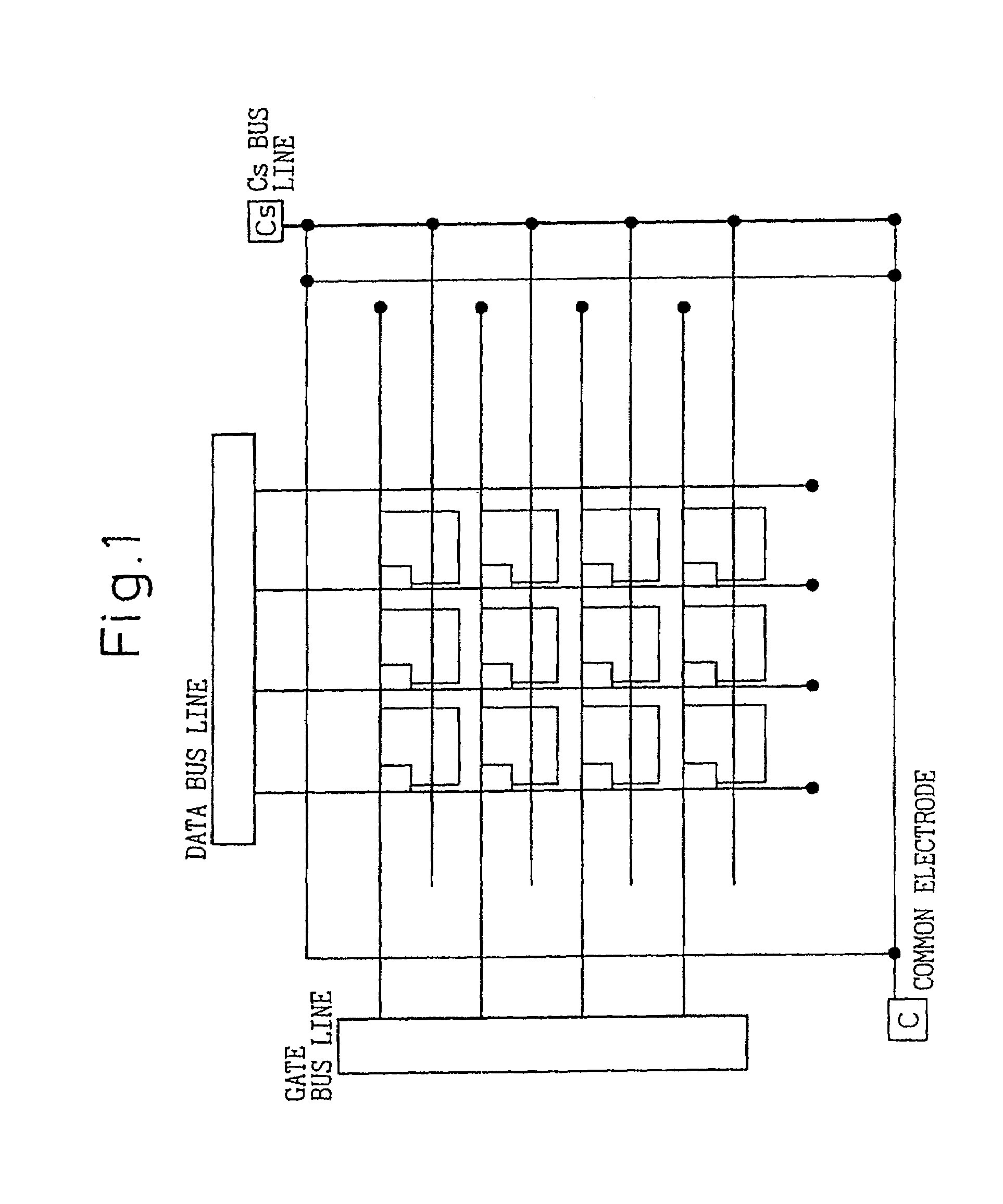
[0257]As shown in FIG. 9, gate bus lines and data bus lines are arranged in an matrix array on a first substrate, and the respective bus lines are bundled at one end. A TFT is located at each intersection of the bus lines, and a pixel electrode is formed via the TFT. On a second substrate on the opposite side is formed a common electrode which forms an electrical capacitance to each of the pixel electrodes, and a pad for applying a voltage to it is drawn out in the lower left corner.

[0258]The pixel electrodes also form a layer called a Cs bus line and an auxiliary capacitance Cs within the first substrate. It can be said that the Cs bus line is another common electrode. The Cs bus line is drawn out as a pad (Cs) in the upper right corner.

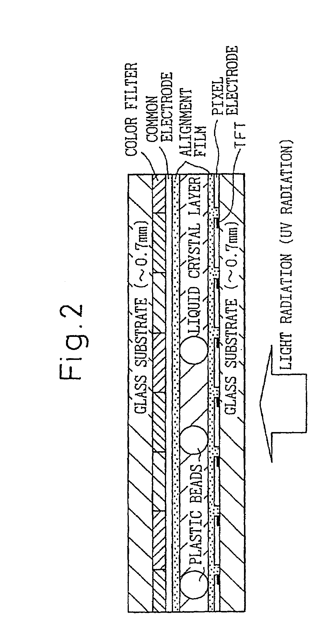
[0259]The cross section of the thus constructed liquid crystal panel is the same as that shown in FIG. 2; here, the first substrate corresponds to the bottom substrate and the second substrate to the substrate on which color filters are deposited.

[0...

embodiment 2

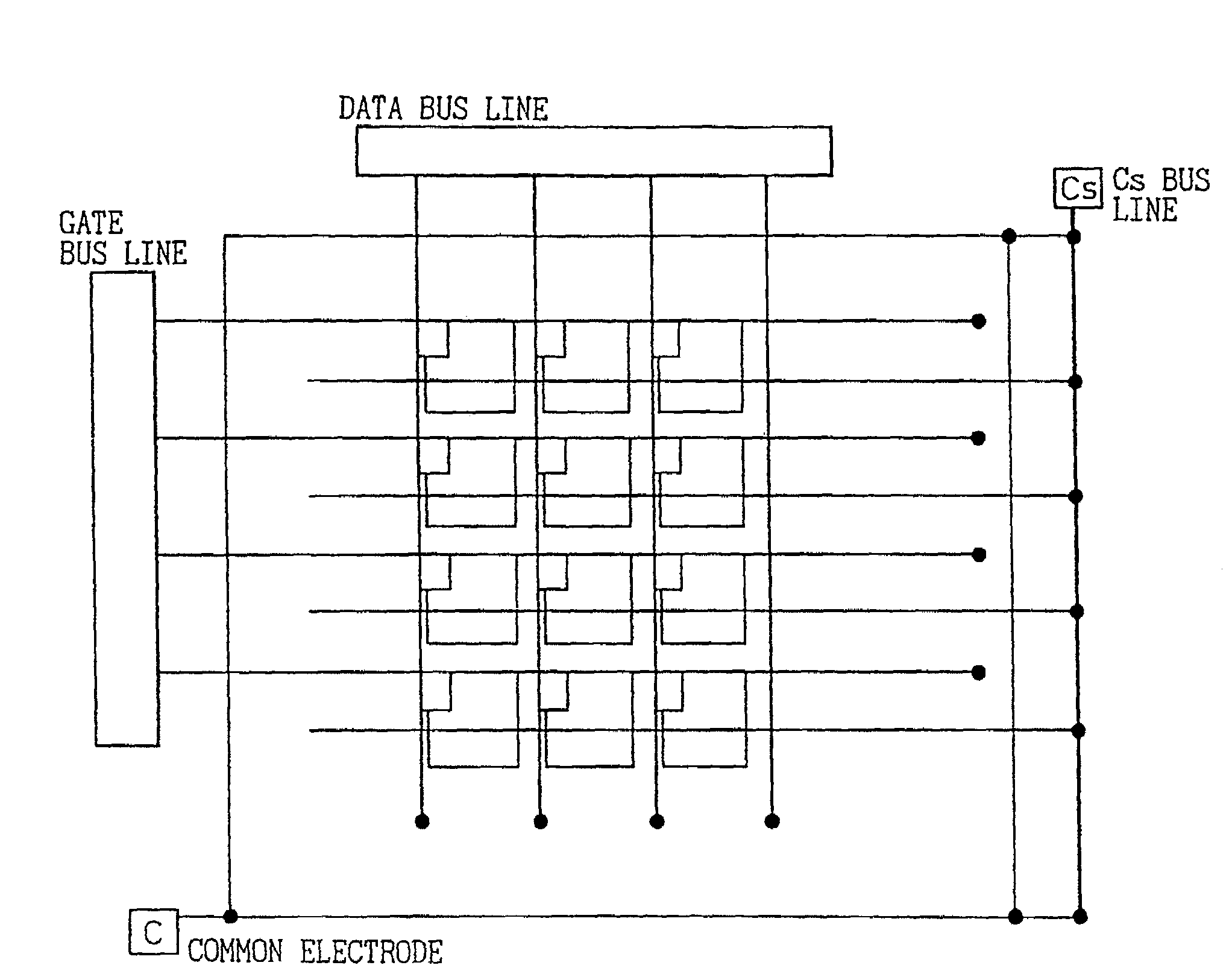
[0264]Compared with the structure of the first embodiment shown in FIG. 1, the common electrode and the Cs bus line are completely insulated from each other in the structure shown in FIG. 12 (generally, they are short-circuited using conductive particles or silver paste).

[0265]It is preferable to completely insulate the common electrode from the Cs bus line as illustrated here, because deterioration of the applied AC voltage can then be alleviated.

[0266]In particular, the resistance per Cs bus line is often of the order of several thousand ohms and, depending on the magnitude of leakage, the applied voltage drops.

embodiment 3

[0267]As described above, it is desirable that the common electrode and the Cs bus line be electrically insulated from each other, considering the voltage application when exposing the liquid crystal to radiation. This method, however, requires that a separate pattern from the voltage supply pattern to the Cs bus line be formed for the common electrode that needs to be supplied with currents from the four sides.

[0268]In view of this, if the common electrode is shorted to the Cs bus line after the radiation, as shown in the example shown here, supply of currents from the four sides can be easily accomplished.

[0269]More specifically, as shown in the example of FIG. 13, portions that can be shorted using a laser are provided in advance within the panel structure. For this purpose, it is generally practiced to electrically connect the top and bottom substrates by using silver paste or conductive spacer means.

[0270]On the other hand, in the example shown in FIG. 14, the connection is mad...


PUM

PropertyMeasurementUnit
polar angleaaaaaaaaaa
AC frequencyaaaaaaaaaa
thicknessaaaaaaaaaa

Abstract

When radiating light onto a liquid crystal composition containing a photosensitive material, the alignment of liquid crystal molecules is adjusted by applying a voltage to the liquid crystal composition layer, to achieve substantially orderly alignment of the liquid crystal molecules, or the alignment of the liquid crystal molecules is made uniform by adjusting the structure of the liquid crystal display device, or any display defect is driven out of the display area. When radiating light to the liquid crystal composition containing the photosensitive material, the alignment of the liquid crystal molecules can be adjusted so as to achieve substantially orderly alignment of the liquid crystal molecules, and the liquid crystal display device can thus be driven stably.

Description

CROSS REFERENCE OF RELATED APPLICATION[0001]This application is a division of application Ser. No. 10 / 893,790, filed Jul. 16, 2004, which is a division of application Ser. No. 10 / 263,257, filed Oct. 2, 2002, which is now U.S. Pat. No. 6,778,229, issued Aug. 17, 2004, which is a continuation-in-part of application Ser. No. 10 / 107,989, filed Mar. 27, 2002, which is now abandonedBACKGROUND OF THE INVENTION[0002]1. Field of the Invention[0003]The present invention relates to a liquid crystal display device to be used for television and other display apparatuses, to a method of fabricating the same and, more particularly, to a liquid crystal display device that uses a liquid crystal material containing a photosensitive material and a method of fabricating the same.[0004]2. Description of the Related Art[0005]A liquid crystal display device is a display device that comprises a liquid crystal sealed between two opposing substrates and that uses electrical stimulus for optical switching by ...

Claims


Application Information

Patent Timeline
Patent Type & Authority Applications(United States)
IPC IPC(8): G02F1/1337G02F1/1341G02F1/1343G02F1/1362G02F1/1368
CPCG02F1/1337G02F1/136213G02F1/1368G02F1/13
Inventor INOUE, HIROYASUNAGAOKA, KENICHINAKAHATA, YUJITANIGUCHI, YOJIFUJIKAWA, TETSUYANAKANISHI, YOHEIHANAOKA, KAZUTAKAINOUE, YUICHISHIBASAKI, MASAKAZU
Owner SHARP KK
Why Eureka
Try Eureka