Semiconductor device and transistor

a technology of semiconductor devices and transistors, applied in the direction of semiconductor devices, basic electric elements, electrical appliances, etc., can solve the problems of increasing manufacturing costs, increase manufacturing costs, etc., and achieve the effect of increasing the impurity concentration of the relevant substrate, increasing the vth of the subchannel, and not increasing the gate capacitan

Inactive Publication Date: 2009-01-01
LONGITUDE SEMICON S A R L
View PDF2 Cites 5 Cited by
  • Summary
  • Abstract
  • Description
  • Claims
  • Application Information

AI Technical Summary

Benefits of technology

[0013]In light of the above circumstances, an object of the present invention is to provide a semiconductor device having a fin-channel structure, and a relevant transistor, by which it is unnecessary to perform ion implantation so as to increase the impurity concentration of the relevant substrate and to increase Vth of the sub channel; the gate capacitance does not increase; and the device speed can be further increased without increasing the manufacturing cost.

Problems solved by technology

However, the relevant processes are complex, which increases the manufacturing cost.

Method used


Image

  • Semiconductor device and transistor
  • Semiconductor device and transistor
  • Semiconductor device and transistor

Examples


Embodiment Construction

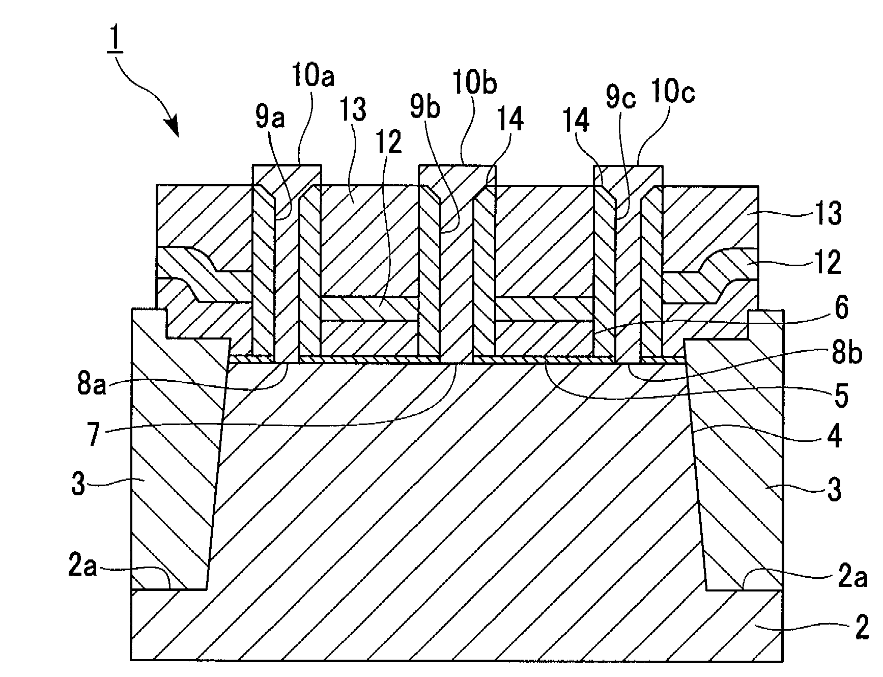
[0064]Hereinafter, a semiconductor device and a relevant transistor, to which the present invention is applied, will be described in detail with reference to the appended figures. In order to show distinctive features in an easily-understandable manner, parts corresponding to the distinctive features may be enlarged in the figures, that is, the dimensional ratio between the shown structure elements may not correspond to the actual ratio therebetween. In addition, materials, sizes, and the like, which are employed in the following embodiment, are just examples, and the present invention is not limited thereto.

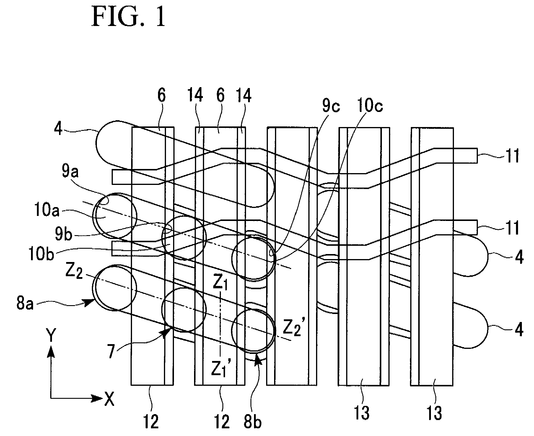
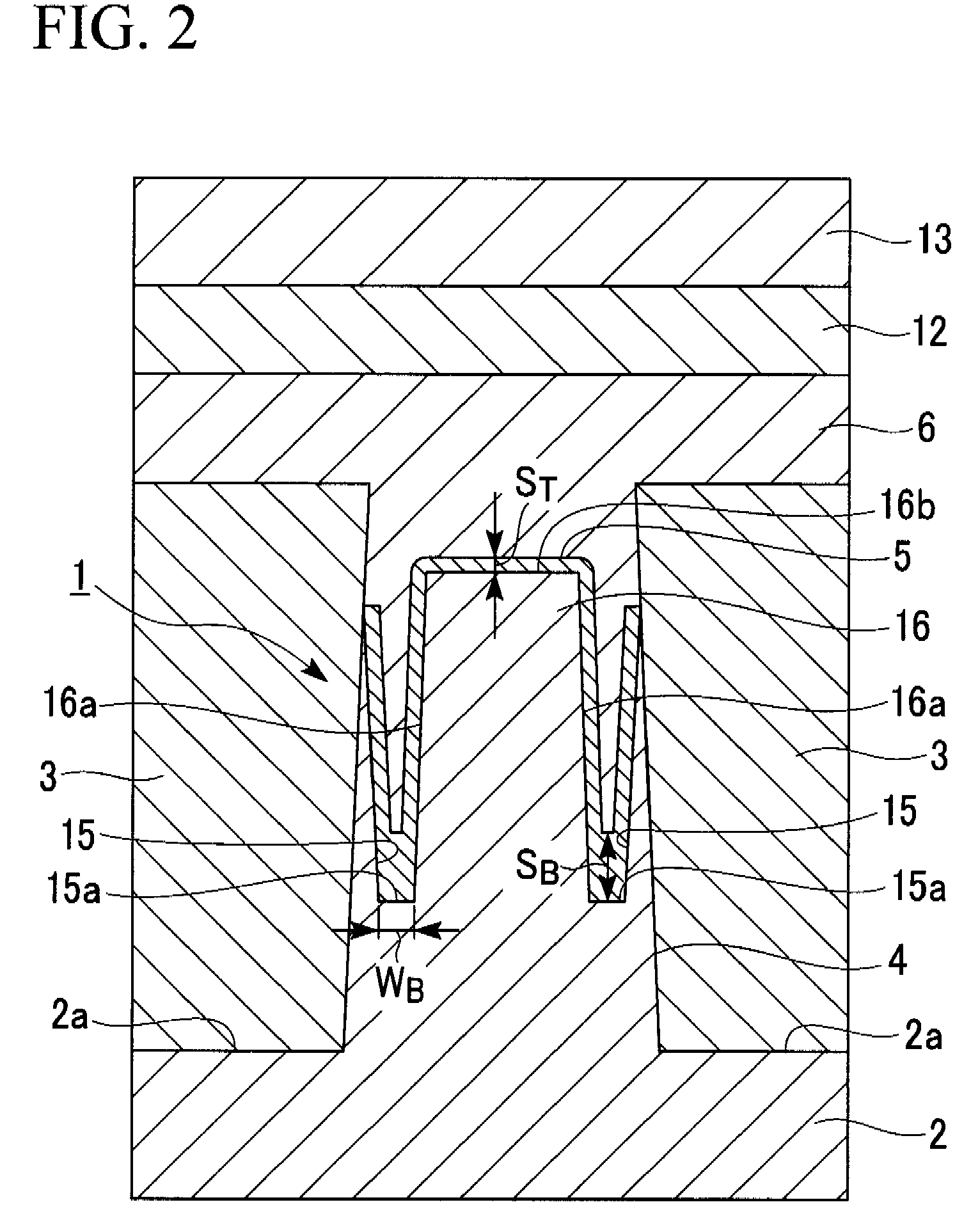
[0065]In the embodiment of the semiconductor device, the present invention is applied to a fin-FET 1 as shown in FIGS. 1 to 3.

[0066]The fin-FET 1 to which the present invention is applied may be used as a transistor for selecting one of memory cells arranged in a cell array area of a DRAM (dynamic random access memory) as shown in FIG. 1, where in the cell array area, a 2-bit me...


PUM


Abstract

A semiconductor device includes active areas which are insulatedly separated from each other by element-separation insulating films; a gate insulating film formed on each active area; a gate electrode which extends across the active area via the gate insulating film; a source area and a drain area formed in the active area so as to interpose the gate electrode; and a fin-channel structure in which at the intersection between the active area and the gate electrode, trenches are provided at both sides of the active area, and part of the gate electrode is embedded in each trench via the gate insulating film, so that the gate electrode extends across a fin which rises between the trenches. In the gate insulating film, the film thickness of a part which contacts the bottom surface of each trench is larger than that of a part which contacts the upper surface of the fin.

Description

BACKGROUND OF THE INVENTION[0001]1. Field of the Invention[0002]The present invention relates to a semiconductor device having a fin-channel structure, and a relevant transistor.[0003]Priority is claimed on Japanese Patent Application No. 2007-167377, filed Jun. 26, 2007, the contents of which are incorporated herein by reference.[0004]2. Description of the Related Art[0005]In accordance with recent progress in fine processing of semiconductor devices, the size of each transistor tends to decrease, which makes a short channel effect of the transistor more remarkable. For example, in a DRAM (dynamic random access memory) or the like, as the channel length of the transistor is also reduced due to a reduction in the memory-cell size, the performance of the transistor is degraded, thereby degrading the data retention and writing performance of the memory cell.[0006]In order to solve such a problem, a recess transistor, a fin-FET (fin-field effect transistor), and the like have been deve...

Claims


Application Information

Patent Timeline
Patent Type & Authority Applications(United States)
IPC IPC(8): H01L29/00
CPCH01L29/66795H01L29/7853H01L29/785
Inventor KAWAKITA, KEIZO
Owner LONGITUDE SEMICON S A R L
Why Eureka
Try Eureka