

Method for Transferring Semiconductor Element, Method for Manufacturing Semiconductor Device, and Semiconductor Device
- Summary
- Abstract
- Description
- Claims
- Application Information
AI Technical Summary
Benefits of technology
Problems solved by technology
Method used
Image

Examples
Embodiment Construction
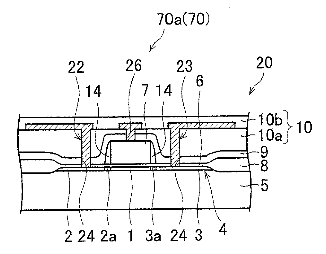
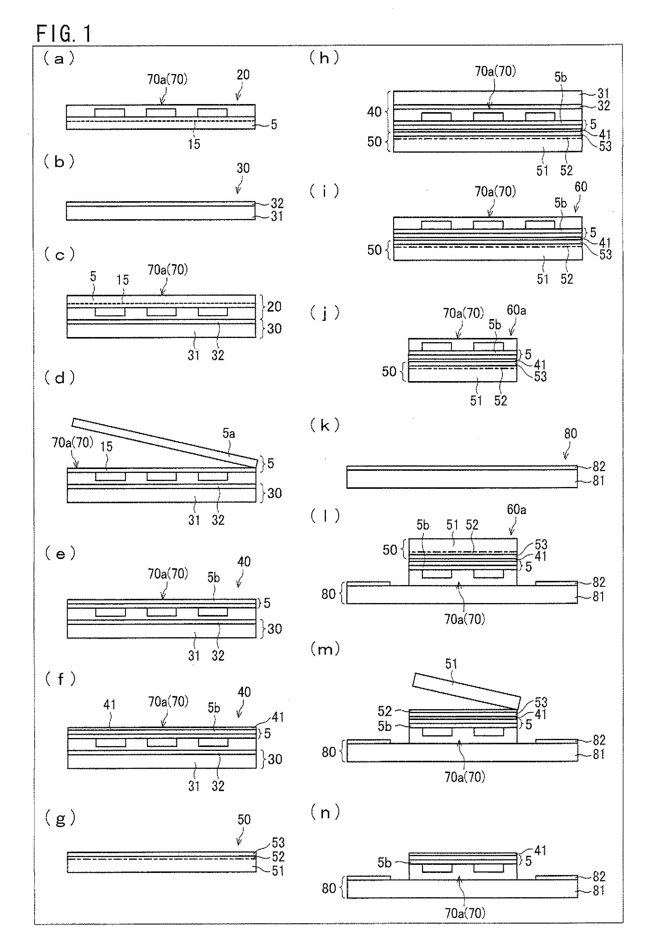
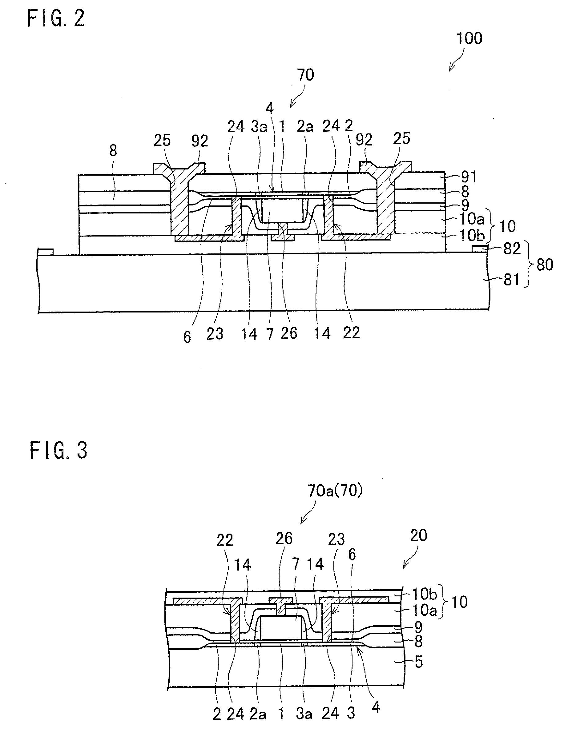
[0082]An embodiment of the present invention is described below with reference to (a) to (n) of FIG. 1 and FIG. 6.
[0083]A semiconductor device of the present invention is a semiconductor device utilizing an insulating substrate having a low heat resistance as a substrate onto which a semiconductor element such as a semiconductor transistor is finally transferred (moved), namely, as a substrate which is finally used for, for example, a display apparatus and is a so-called production substrate. The insulating substrate is a substrate such as a glass substrate and has been conventionally difficult to apply.
[0084]In the present embodiment, described below as an example of the semiconductor device of the present embodiment is a semiconductor device having a structure in which a chip-type semiconductor transistor, which is the semiconductor element above, has been transferred onto a substrate formed (TFT substrate) on which a pixel area has been formed. However, the present invention is n...
PUM
 Abstract
Description
Claims
Application Information