Multilayer ceramic capacitor with internal current cancellation and bottom terminals

Active Publication Date: 2009-01-01
KYOCERA AVX COMPONENTS CORP
View PDF53 Cites 35 Cited by
  • Summary
  • Abstract
  • Description
  • Claims
  • Application Information

AI Technical Summary

Benefits of technology

[0024]Various additional objects and advantages are provided by present embodiments which adhere to the present exemplary features that the current loop area should be minimized by a) minimizing the gap between the opposing polarity internal electrode tabs, b) matching the external termination to the expos

Problems solved by technology

As switching speeds increase and pulse rise times decrease in electronic circuit applications, the need to reduce inductance becomes a serious limitation for improved system performance.
Even the decoupling capacitors, that act as a local energy source, can generate una

Method used


Image

  • Multilayer ceramic capacitor with internal current cancellation and bottom terminals
  • Multilayer ceramic capacitor with internal current cancellation and bottom terminals
  • Multilayer ceramic capacitor with internal current cancellation and bottom terminals

Examples


Embodiment Construction

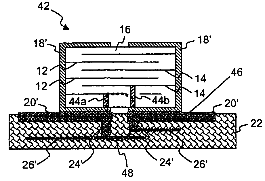
[0087]The present subject matter is directed towards improved component design for decoupling capacitors that selectively incorporates closely spaced termination gaps and / or vertically oriented electrodes to provide parts with relatively low inductance and low ESR.

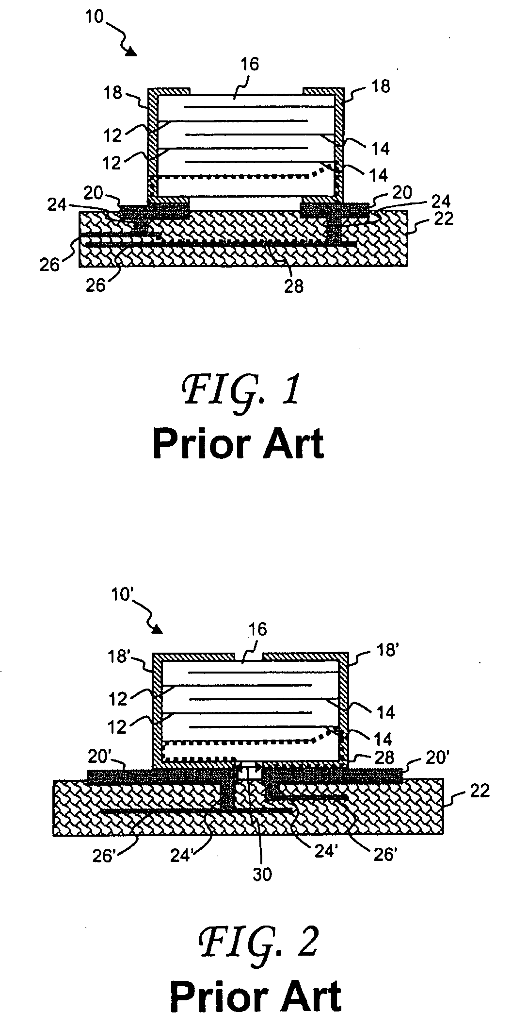
[0088]As referenced in the Background of the Invention section, supra, many known systems and methods have been directed to the formation of multilayer electronic components characterized by low inductance and / or low ESR values. Examples of such known technologies include components that incorporate one or more of a reverse geometry termination, interdigitated capacitor electrodes, or ball grid arrays with alternating current flow in adjacent electrodes. Central to each of the aforementioned approaches is a goal to minimize the area of the current carrying loop formed between the capacitor and its mounting location. Assuming that a mounting location corresponds to a conventional circuit board, such a current carrying loop ...


PUM

PropertyMeasurementUnit
Electrical conductoraaaaaaaaaa

Abstract

Low inductance capacitors include electrodes that are arranged among dielectric layers and oriented such that the electrodes are substantially perpendicular to a mounting surface. Vertical electrodes are exposed along a device periphery to determine where termination lands are formed, defining a narrow and controlled spacing between the lands that is intended to reduce the current loop area, thus reducing the component inductance. Further reduction in current loop area and thus component equivalent series inductance (ESL) may be provided by interdigitated terminations. Terminations may be formed by various electroless plating techniques, and may be directly soldered to circuit board pads. Terminations may also be located on “ends” of the capacitors to enable electrical testing or to control solder fillet size and shape. Two-terminal devices may be formed as well as devices with multiple terminations on a given bottom (mounting) surface of the device. Terminations may also be formed on the top surface (opposite a designated mounting surface) and may be a mirror image, reverse-mirror image, or different shape relative to the bottom surface.

Description

PRIORITY CLAIM[0001]This application claims the benefit of priority as a continuation-in-part application of previously filed U.S. Utility Patent Application entitled “MULTILAYER CERAMIC CAPACITOR WITH INTERNAL CURRENT CANCELLATION AND BOTTOM TERMINALS”, filed Oct. 26, 2006 and assigned U.S. Ser. No. 11 / 588,104, which application claims priority to U.S. Provisional Patent Application entitled “LOW INDUCTANCE CAPACITOR WITH EXTENDED LANDS AND VERTICAL ELECTRODES”, filed Oct. 31, 2005 and assigned U.S. Ser. No. 60 / 731,811. The complete disclosures of the foregoing applications are fully incorporated herein by reference for all purposes; priority is claimed to all of the above-referenced applications.BACKGROUND OF THE INVENTION[0002]The present subject matter generally concerns improved component design for decoupling capacitors that generally results in devices characterized by relatively low cost, low inductance and low Equivalent Series Resistance (ESR).[0003]As switching speeds inc...

Claims


Application Information

Patent Timeline
IPC IPC(8): H01G4/12
CPCH01C1/148H01C7/18H01G2/065H01G4/012Y10T29/435H01G4/30H05K1/0231H05K1/113H05K2201/0792H01G4/232H01G4/228
Inventor RITTER, ANDREW P.GALVAGNI, JOHN L.
Owner KYOCERA AVX COMPONENTS CORP
Why Eureka
Try Eureka