Semiconductor Light Emitting Device Member, Method for Manufacturing Such Semiconductor Light Emitting Device Member and Semiconductor Light Emitting Device Using Such Semiconductor Light Emitting Device Member

Active Publication Date: 2009-01-08
MITSUBISHI CHEM CORP
View PDF1 Cites 118 Cited by
  • Summary
  • Abstract
  • Description
  • Claims
  • Application Information

AI Technical Summary

Benefits of technology

[0056]A semiconductor light-emitting device member according to the present invention can be coated as a thick film compared with a conventional inorganic member for semiconductor light-emitting device, and is capable of easily sealing a semiconductor light-emitting device

Problems solved by technology

However, due to high hygroscopicity of epoxy resin, there have been problems of cracks caused by heat from a semiconductor luminous element when the semiconductor light-emitting device is used for a long time and degradation of the phosphor and luminous element caused by moisture infiltration.
Also in recent years, as the luminous wave

Method used


Image

  • Semiconductor Light Emitting Device Member, Method for Manufacturing Such Semiconductor Light Emitting Device Member and Semiconductor Light Emitting Device Using Such Semiconductor Light Emitting Device Member
  • Semiconductor Light Emitting Device Member, Method for Manufacturing Such Semiconductor Light Emitting Device Member and Semiconductor Light Emitting Device Using Such Semiconductor Light Emitting Device Member
  • Semiconductor Light Emitting Device Member, Method for Manufacturing Such Semiconductor Light Emitting Device Member and Semiconductor Light Emitting Device Using Such Semiconductor Light Emitting Device Member

Examples


embodiment a-1

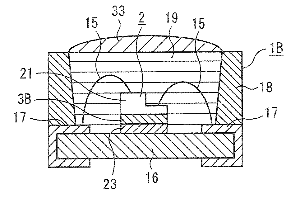
[0745]In the luminescent device 1A in the present embodiment, as shown in FIG. 1, the luminous element 2 is surface-mounted on an insulating substrate 16 on which printed wiring 17 is carried out. In the luminous element 2, a p-type semiconductor layer (not shown) and an n-type semiconductor layer (not shown) in a luminous layer part 21 are connected electrically to the printed wiring 17 and 17 via conductive wires 15 and 15 respectively. The conductive wires 15 and 15 have a small cross section so that light emitted from the luminous element 2 should not be blocked.

[0746]Any luminous element 2 that emits light of wavelengths from ultraviolet to infrared regions may be used, but here a gallium nitride LED chip is assumed to be used. In the luminous element 2, the n-type semiconductor layer (not shown) is formed on a lower side in FIG. 1 and the p-type semiconductor layer (not shown) is formed on an upper side, and the upper side of FIG. 1 is assumed to a front for a description belo...

embodiment a-2

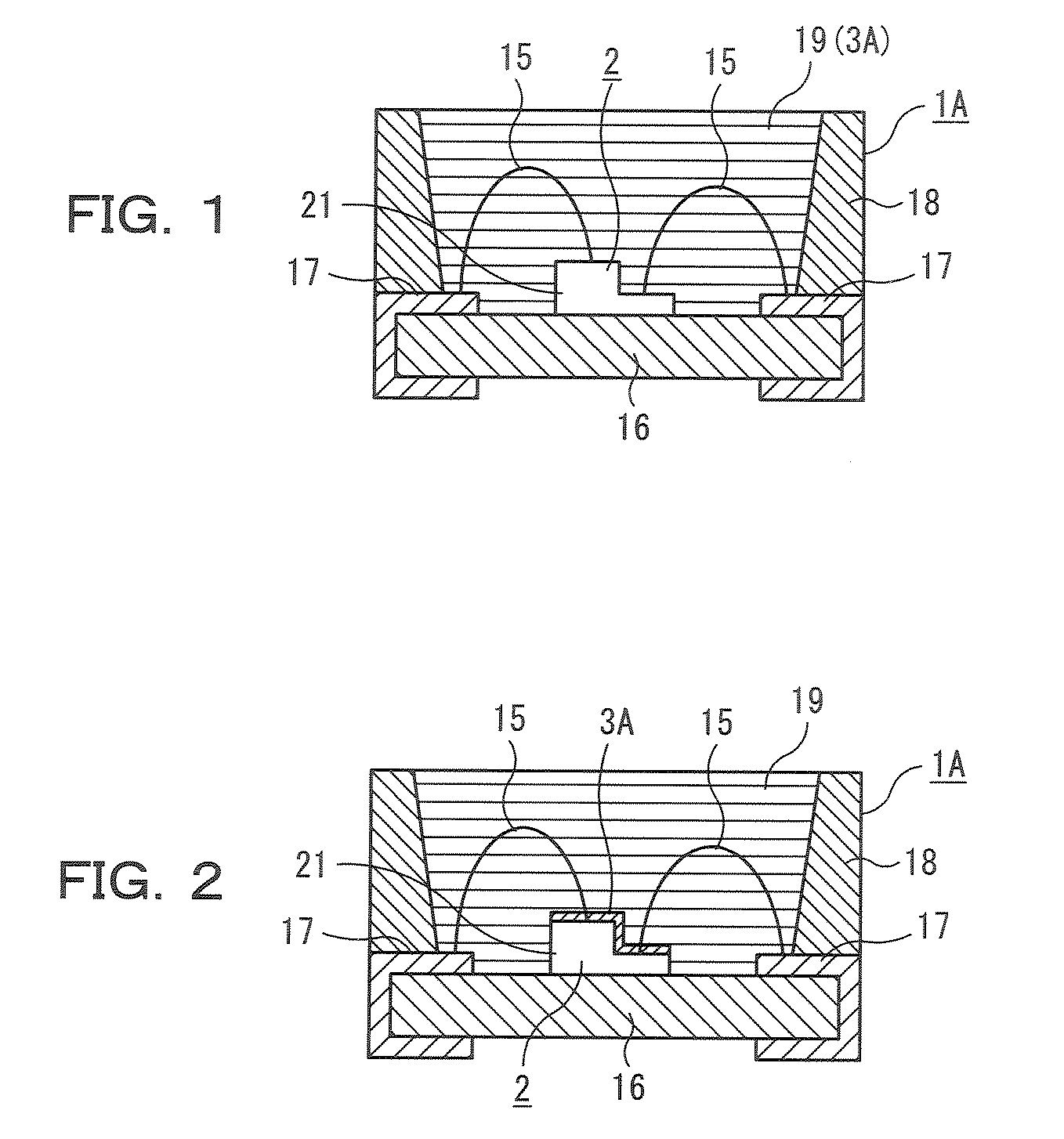
[0750]The luminescent device 1A in the present embodiment is structured, as shown in FIG. 2, in the same manner as the above embodiment A-1 except that the front of the luminous element 2 is covered with the transparent member 3A and the sealing part 19 is formed thereupon with a material different from that of the transparent member 3A. The transparent member 3A on the surface of the luminous element 2 is a transparent thin film functioning as a light extracting film and sealing film and can be formed, for example, by coating the above semiconductor light-emitting device member formation liquid using a spin coating when a chip of the luminous element 2 is formed. Meanwhile, the same numeral is attached to the same component as in the embodiment A-1 to omit a description thereof.

[0751]Thus, like the embodiment A-1, the luminescent device 1A in the present embodiment is provided with the luminous element 2 and transparent member 3A, and thus light durability and heat resistance of th...

embodiment b-1

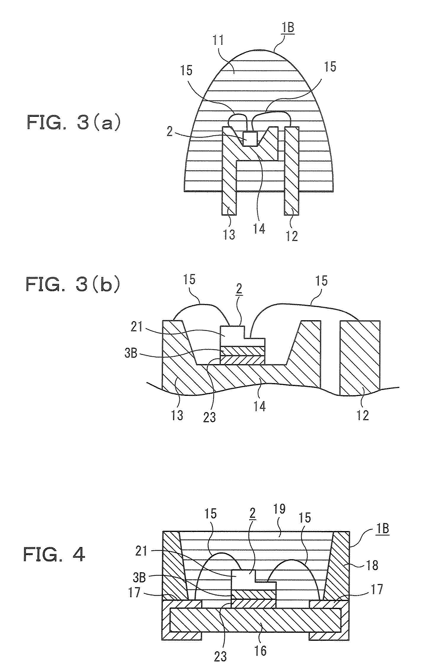
[0752]The luminescent device 1B in the present embodiment is provided, as shown in FIG. 3(a), with the luminous element 2 comprised of an LED chip and a mold part 11 obtained by forming a translucent transparent material into a cannonball shape. The mold part 11 covers the luminous element 2 and the luminous element 2 is electrically connected to lead terminals 12 and 13 formed of conductive material. The lead terminals 12 and 13 are formed of a lead frame.

[0753]In the luminous element 2, which is a gallium nitride LED chip, an n-type semiconductor layer (not shown) is formed on the lower side in FIG. 3(a) and a p-type semiconductor layer (not shown) is formed on the upper side, and the upper side of FIG. 3(a) and FIG. 3(b) is assumed to the front for a description below because light output is extracted from the p-type semiconductor layer side. A rear surface of the luminous element 2 is joined to a mirror (cup surface) 14 attached to a front end part of the lead by die bonding. Th...


PUM

PropertyMeasurementUnit
Temperatureaaaaaaaaaa
Fractionaaaaaaaaaa
Fractionaaaaaaaaaa

Abstract

A semiconductor light-emitting device member excellent in transparency, light resistance, and heat resistance and capable of sealing a semiconductor light-emitting device without causing cracks and peeling even after a long-time use is provided. Therefore, a semiconductor light-emitting device member that comprises (1) in a solid Si-nuclear magnetic resonance spectrum, at least one peak selected from a group consisting of (i) peaks whose peak top position is in an area of a chemical shift of −40 ppm to 0 ppm inclusive, and whose full width at half maximum is 0.3 ppm to 3.0 ppm inclusive, and (ii) peaks whose peak top position is in an area of the chemical shift of −80 ppm or more and less than −40 ppm, and whose full width at half maximum is 0.3 ppm to 5.0 ppm inclusive, wherein (2) silicon content is 20 weight % or more and (3) silanol content is 0.1 weight % to 10 weight % inclusive is used.

Description

TECHNICAL FIELD[0001]The present invention relates to a novel semiconductor light-emitting device member, a manufacturing method therefor, and a semiconductor light-emitting device using thereof. More particularly, the present invention relates to a semiconductor light-emitting device member having high ultraviolet ray and heat resistance and excellent in transparency, a manufacturing method therefor, and a semiconductor light-emitting device using thereof.BACKGROUND ART[0002]In a semiconductor light-emitting device such as a light-emitting diode (hereinafter called “LED” when appropriate) and semiconductor laser, a semiconductor luminous element is generally sealed by a member (semiconductor light-emitting device member) such as transparent resin.[0003]Epoxy resin, for example, is used as a semiconductor light-emitting device member. It is also known that a luminous wavelength from a semiconductor luminous element is converted by making the sealing resin contain a pigment such as a...

Claims


Application Information

Patent Timeline
IPC IPC(8): H01L33/00H01L21/00H01L33/56
CPCC08G77/04H01L33/56H01L2224/48091H01L2224/49107H01L2224/45144H01L2924/00014H01L2924/00
Inventor KATO, HANAKOMORI, YUTAKAKOBAYASHI, HIROSHITOMURA, TSUBASA
Owner MITSUBISHI CHEM CORP
Why Eureka
Try Eureka