Electronic Component With P-Doped Organic Semiconductor

a technology of organic semiconductors and electronic components, applied in the direction of discharge tubes luminescnet screens, conductors, non-metal conductors, etc., can solve the problems of general toxicity of organic p-dopants, and achieve the effect of limiting ohmic losses in the diod

Active Publication Date: 2009-01-15
COMMISSARIAT A LENERGIE ATOMIQUE ET AUX ENERGIES ALTERNATIVES
View PDF14 Cites 5 Cited by
  • Summary
  • Abstract
  • Description
  • Claims
  • Application Information

AI Technical Summary

Benefits of technology

[0019]The thickness of said p-doped organic semiconducting material layer is preferably higher than or equal to 30 nm. If the hole transporting layer comprises a p-doped part and a non p-doped part, only the thickness of the doped part is taken into account here. The thickness of this layer is preferably less than or equal to 100 nm, in particular to limit ohmic losses in the diode.

Problems solved by technology

The p-dopants that are usually suitable are generally organic dopants, such as F4-TCNQ; these organic p-dopants are generally toxic.

Method used


Image

  • Electronic Component With P-Doped Organic Semiconductor
  • Electronic Component With P-Doped Organic Semiconductor

Examples


Embodiment Construction

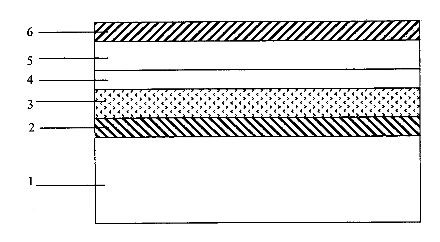
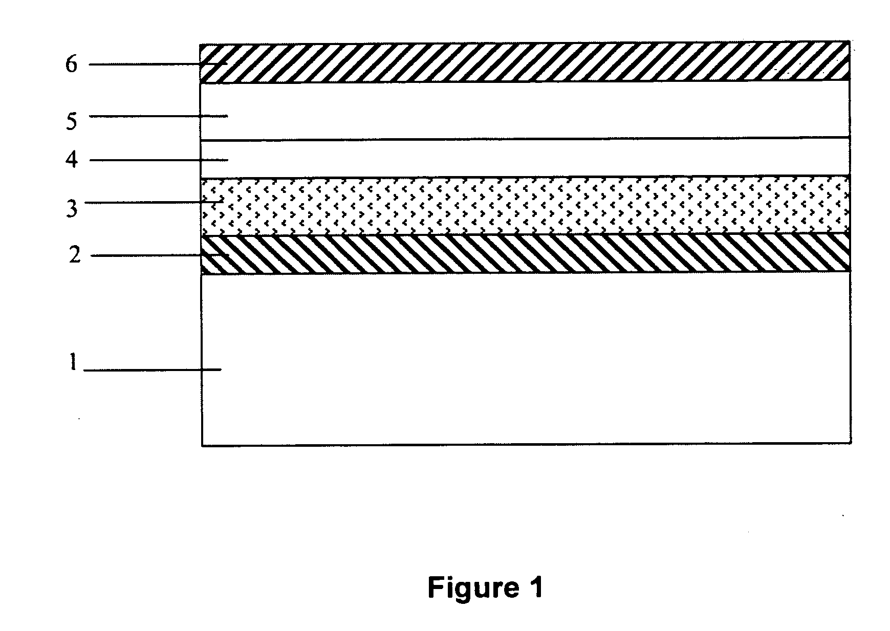
[0020]The invention will be better understood on reading the following description, given for non-restrictive example purposes only with reference to appended FIG. 1, which represents an organic light-emitting diode structure according to an embodiment of the invention. The invention is applicable to any other electronic component.

[0021]With reference to FIG. 1, an anode 2 is deposited on an insulating substrate 1. The anode is for example made from ITO, whose work function is equal to 4.7 eV; Deposition is performed in conventional manner, for example by cathode sputtering in vacuum.

[0022]A layer 3 of p-doped organic semiconducting material designed to serve the purpose of transporting holes is then deposited. Deposition is performed by co-evaporation in vacuum of this organic semiconducting material and of the p-dopant which is here an inorganic chemical element having an ionization potential higher than or equal to 4.7 eV; cobalt or nickel are for example used; unlike the p-dopin...


PUM

PropertyMeasurementUnit
HOMOaaaaaaaaaa
pressureaaaaaaaaaa
thicknessaaaaaaaaaa

Abstract

An electronic component comprising a layer of organic semiconducting material in which a dopant is dispersed having an energy difference between the work function of the dopant and of the HOMO level of said organic semiconducting material that is less than 0.5 eV. The dopant is an atomic element having an evaporation temperature lower than 1300° C. for a pressure of 10−8 Torr. The invention enables the toxicity problems connected with usual organic acceptor dopants to be avoided. It applies in particular to organic light-emitting diodes.

Description

BACKGROUND OF THE INVENTION[0001]The invention relates to p-doping of organic semiconducting materials having a base in particular formed by small molecules (as opposed to polymers), and to the use of these doped semiconductors in particular for light-emitting diodes, organic transistors, or for any other electronic component. The p-dopants are electron acceptor dopants; they are therefore generally oxidative with regard to the material they dope.STATE OF THE ART[0002]Fabrication of transistors or diodes with an organic semiconductor having a base formed by small molecules generally requires a vacuum deposition step on a substrate generally previously provided with one or more electrodes called bottom electrodes; in this step, the semiconductor molecule is evaporated in a vacuum chamber so that it recondenses on this substrate to form a deposition layer; one or more electrodes called top electrodes are then generally deposited on the organic layer.[0003]The document U.S. Pat. No. 6,...

Claims


Application Information

Patent Timeline
Patent Type & Authority Applications(United States)
IPC IPC(8): H01J1/63B32B9/00H01L51/00
CPCH01L51/002H01L51/5088H01L51/105H10K71/30H10K10/84H10K50/17Y10S428/917
Inventor BEN KHALIFA, MOHAMEDVAUFREY, DAVID
Owner COMMISSARIAT A LENERGIE ATOMIQUE ET AUX ENERGIES ALTERNATIVES
Why Eureka
Try Eureka