Boron derived materials deposition method

a technology of boron-derived materials and deposition methods, which is applied in the field of forming films on substrates, can solve the problems of increasing the power consumed by the gate, destroying the transistor, and affecting the device geometries

Inactive Publication Date: 2009-01-15
APPLIED MATERIALS INC
View PDF9 Cites 66 Cited by
  • Summary
  • Abstract
  • Description
  • Claims
  • Application Information

AI Technical Summary

Problems solved by technology

The continued reduction in device geometries and the increasingly dense spacing of devices on semiconductor substrates have presented challenges in the area of improving device performance.
A very thin gate dielectric may also increase gate leakage that increases the amount of power consumed by the gate and eventually damages the transistor.

Method used


Image

  • Boron derived materials deposition method
  • Boron derived materials deposition method
  • Boron derived materials deposition method

Examples


Embodiment Construction

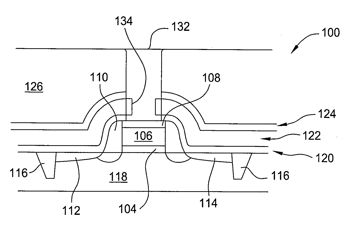
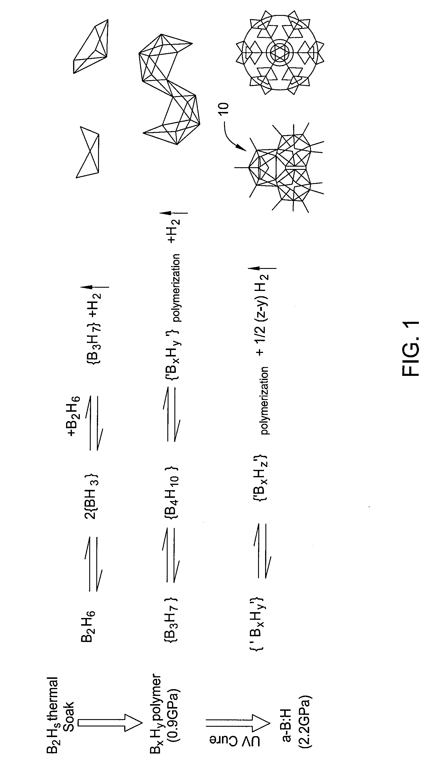
[0019]Embodiments of the present invention provide methods of depositing boron-containing films, such as boron nitride and boron carbide films, for example. The boron-containing films may be undoped boron nitride (BN), undoped boron carbide (BC) films, or doped boron nitride or boron carbide films, such as boron silicon nitride (BSiN), boron carbon nitride (BCN), silicon boron nitride (SiBN) and boron carbon silicon nitride (BCSiN) films. The boron-containing films have a high intrinsic stress, i.e., between about −10 GPa and about 10 GPa, such as a tensile stress that is greater than about 2.0 GPa. It is believed that the high stress of the films is provided at least in part by the presence of B12 icosahedrons within the films. The boron content of the boron-containing films having a high tensile stress, i.e., a stress greater than about 2.0 GPa, may be between about 5 atomic % and about 100 atomic %. The tensile stress typically increases with the boron content.

[0020]Boron-Contain...


PUM

PropertyMeasurementUnit
feature sizesaaaaaaaaaa
tensile stressaaaaaaaaaa

Abstract

Methods of forming boron-containing films are provided. The methods include introducing a boron-containing precursor into a chamber and depositing a network comprising boron-boron bonds on a substrate by thermal decomposition or a plasma process. The network may be post-treated to remove hydrogen from the network and increase the stress of the resulting boron-containing film. The boron-containing films have a stress between about −10 GPa and 10 GPa and may be used as boron source layers or as strain-inducing layers.

Description

CROSS-REFERENCE TO RELATED APPLICATIONS[0001]This application claims benefit of U.S. Provisional Patent Application Ser. No. 60 / 949,796 (Attorney Docket No. 012071L), filed Jul. 13, 2007, which is herein incorporated by reference.BACKGROUND OF THE INVENTION[0002]1. Field of the Invention[0003]Embodiments of the present invention generally relate to methods of forming films on substrates, such as semiconductor substrates. More particularly, embodiments of the present invention relate to methods for forming boron-containing films on substrates.[0004]2. Description of the Related Art[0005]Integrated circuit geometries have dramatically decreased in size since such devices were first introduced several decades ago. Since then, integrated circuits have generally followed the two year / half-size rule (often called Moore's Law), which means that the number of devices on a chip doubles every two years. Today's fabrication facilities are routinely producing devices having 90 nm feature sizes,...

Claims


Application Information

Patent Timeline
Patent Type & Authority Applications(United States)
IPC IPC(8): H01L21/469B05D3/02H05H1/00C08F2/46
CPCC23C16/28C23C16/56H01L21/314H01L21/76814H01L29/7843H01L21/76831H01L21/76832H01L29/6659H01L29/7833H01L21/76826H01L21/02107
Inventor HUH, JEONG-UKBALSEANU, MIHAELAXIA, LI-QUNWITTY, DEREK R.M'SAAD, HICHEM
Owner APPLIED MATERIALS INC
Why Eureka
Try Eureka