Method of manufacturing semiconductor active layer, method of manufacturing thin film transistor using the same and thin film transistor having semiconductor active layer

a manufacturing method and active layer technology, applied in semiconductor devices, vacuum evaporation coatings, coatings, etc., can solve the problems of low mobility layer used in drive circuits of display panels that require a fast response time, leakage current may occur in amorphous silicon or polysilicon semiconductor layers, and may not be uniform

Active Publication Date: 2009-01-22
SAMSUNG DISPLAY CO LTD
View PDF4 Cites 50 Cited by
  • Summary
  • Abstract
  • Description
  • Claims
  • Application Information

AI Technical Summary

Problems solved by technology

The use of such a low mobility layer as a drive circuit of a display panel that requires a fast response time may be difficult.
Polysilicon may be used as the semiconductor layer to provide high mobility, but the threshold voltage of the TFT may not be uniform.
Additionally, leakage current may occur in the amorphous silicon or polysilicon semiconductor layer when light, e.g., light from a backlight unit, is incident thereon.

Method used


Image

  • Method of manufacturing semiconductor active layer, method of manufacturing thin film transistor using the same and thin film transistor having semiconductor active layer
  • Method of manufacturing semiconductor active layer, method of manufacturing thin film transistor using the same and thin film transistor having semiconductor active layer
  • Method of manufacturing semiconductor active layer, method of manufacturing thin film transistor using the same and thin film transistor having semiconductor active layer

Examples


examples

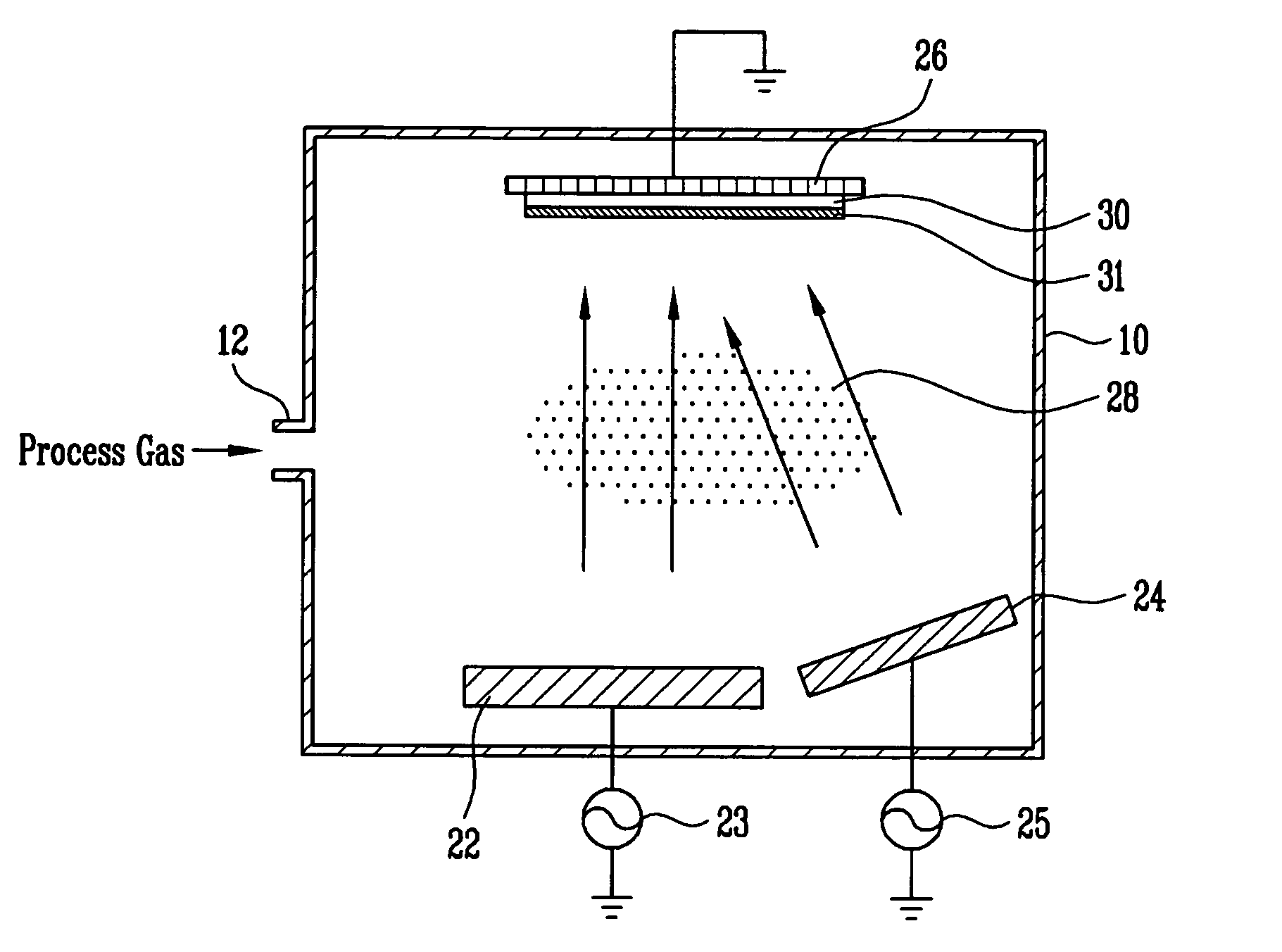
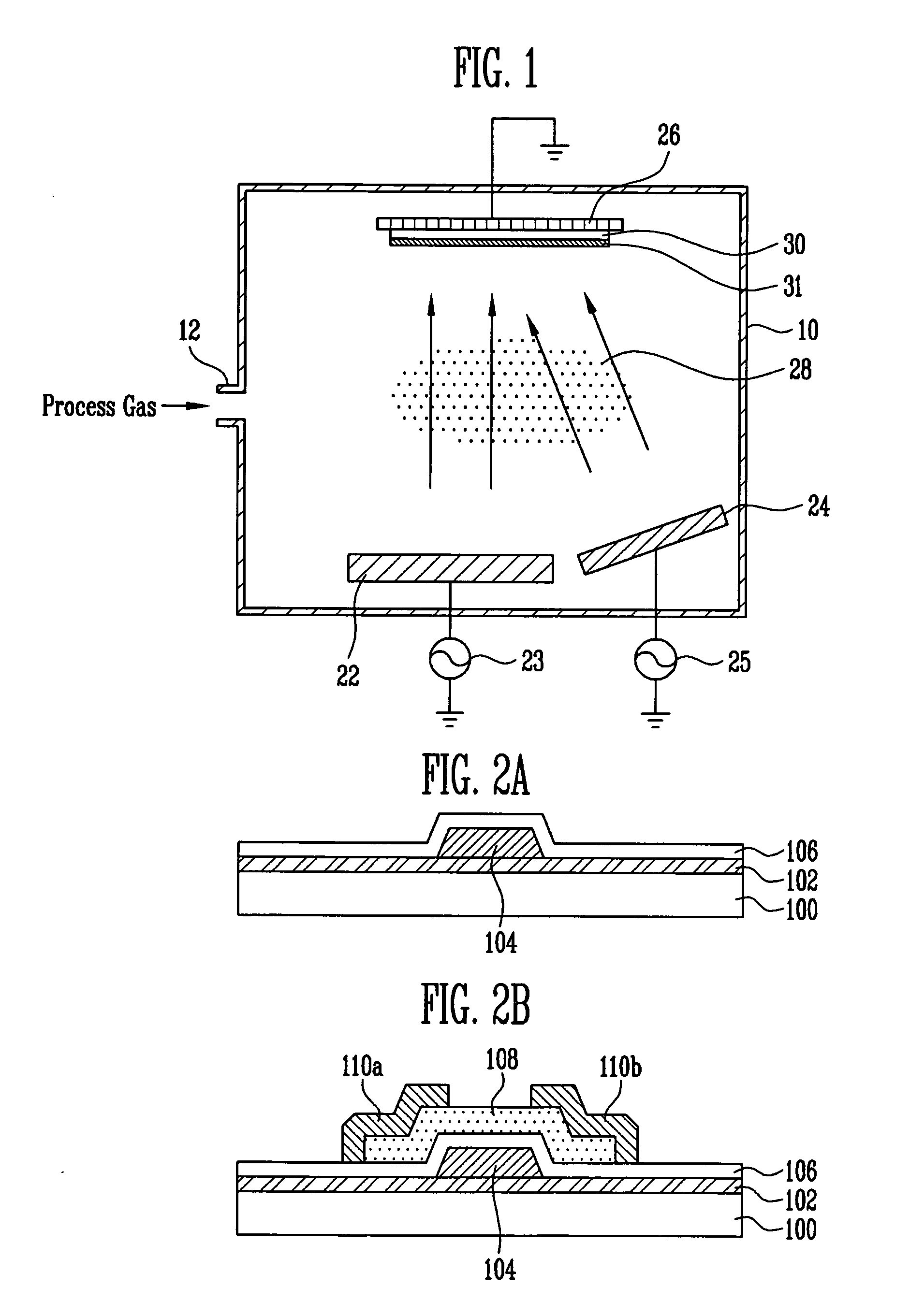
[0048]A buffer layer was formed as a silicon oxide film (SiOx) on a glass substrate, and 200 nm-thick tungsten molybdenum (MoW) was deposited thereon and then patterned to form a gate electrode on the buffer layer. The lateral dimensions of the gate electrode were 70 mm×70 mm.

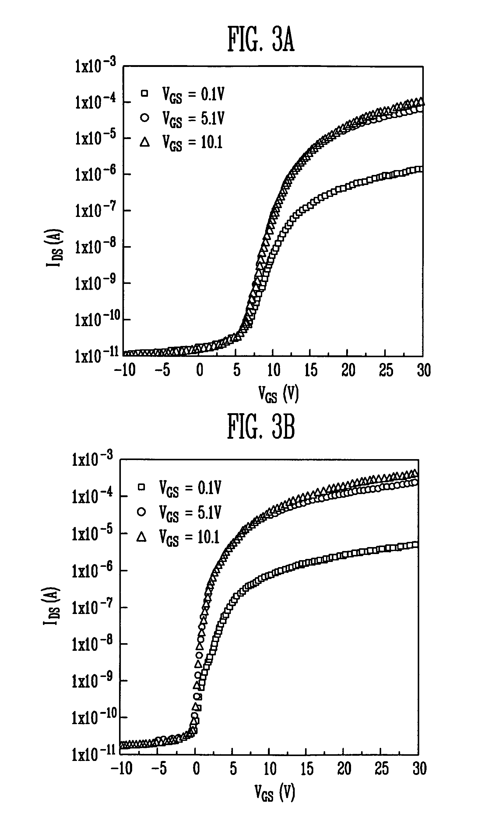
[0049]A 200 nm-thick silicon nitride film (SiNx) was deposited at a temperature of 330° C. using a plasma-enhanced chemical vapor deposition (PECVD) operation to form a gate insulator on the buffer layer and on the gate electrode. An IGZO active layer was formed on the gate insulator in an ambient temperature using a cosputtering apparatus. An amorphous phase of the IGZO active layer was formed having a thickness of 50 nm. The width and length of the channel region of the active layer were 1000 μm and 150 μm, respectively.

[0050]A first target of In2Ga2ZnO7, i.e., InGaZnO, and a second target of In2O3-10 wt % ZnO (90 weight % In2O3 and 10 weight % ZnO), i.e., InZnO, were used to form the IGZO active layer. The i...


PUM

PropertyMeasurementUnit
molar ratiosaaaaaaaaaa
molar ratioaaaaaaaaaa

Abstract

A method of manufacturing an IGZO active layer includes depositing ions including In, Ga, and Zn from a first target, and depositing ions including In from a second target having a different atomic composition from the first target. The deposition of ions from the second target may be controlled to adjust an atomic % of In in the IGZO layer to be about 45 atomic % to about 80 atomic %.

Description

BACKGROUND OF THE INVENTION[0001]1. Field of the Invention[0002]Embodiments relate to a method of manufacturing a semiconductor active layer, a method of manufacturing a thin film transistor using the same, and a thin film transistor including the semiconductor active layer.[0003]2. Description of the Related Art[0004]A semiconductor layer using amorphous silicon or polysilicon has recently been developed for use in a thin film transistor (TFT) for light emitting display devices such as organic light emitting display devices, which use organic light emitting diodes (OLEDs) to emit light.[0005]When the semiconductor layer is formed of amorphous silicon, the semiconductor layer may exhibit low mobility. The use of such a low mobility layer as a drive circuit of a display panel that requires a fast response time may be difficult. Polysilicon may be used as the semiconductor layer to provide high mobility, but the threshold voltage of the TFT may not be uniform. Additionally, leakage cu...

Claims


Application Information

Patent Timeline
Patent Type & Authority Applications(United States)
IPC IPC(8): H01L29/12C23C14/00H01L21/00
CPCC23C14/086C23C14/3464H01L21/02631H01L21/02554H01L21/02565H01L21/02422H01L29/7869
Inventor JEONG, JONG-HANJEONG, JAE-KYEONGPARK, JIN-SEONGMO, YEON-GONYANG, HUI-WONKIM, MIN-KYUAHN, TAE-KYUNGSHIN, HYUN-SOOLEE, HUN JUNG
Owner SAMSUNG DISPLAY CO LTD
Why Eureka
Try Eureka