

Light-emitting device
- Summary
- Abstract
- Description
- Claims
- Application Information
AI Technical Summary
Benefits of technology
Problems solved by technology
Method used
Image

Examples
embodiment mode 1
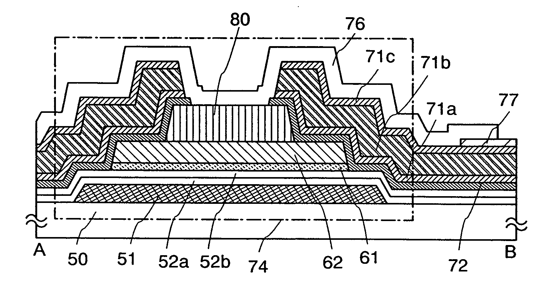
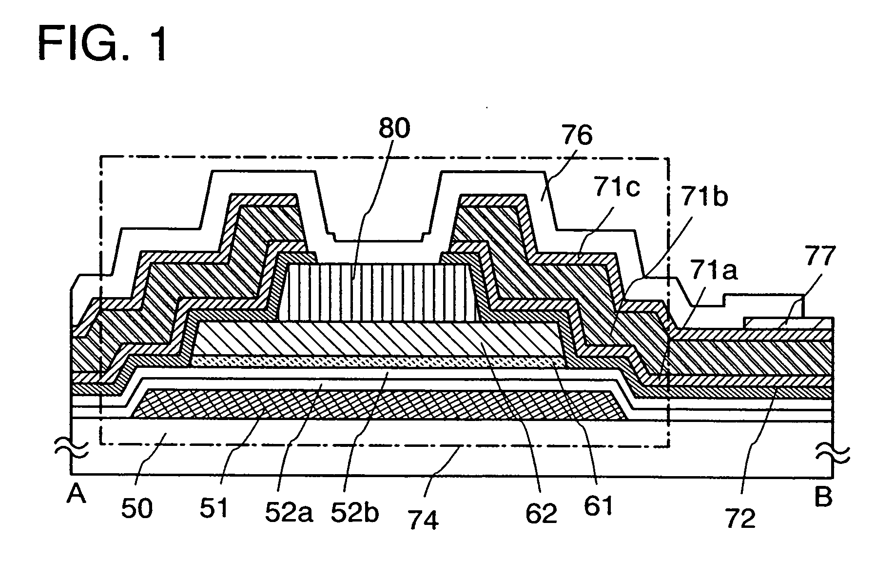
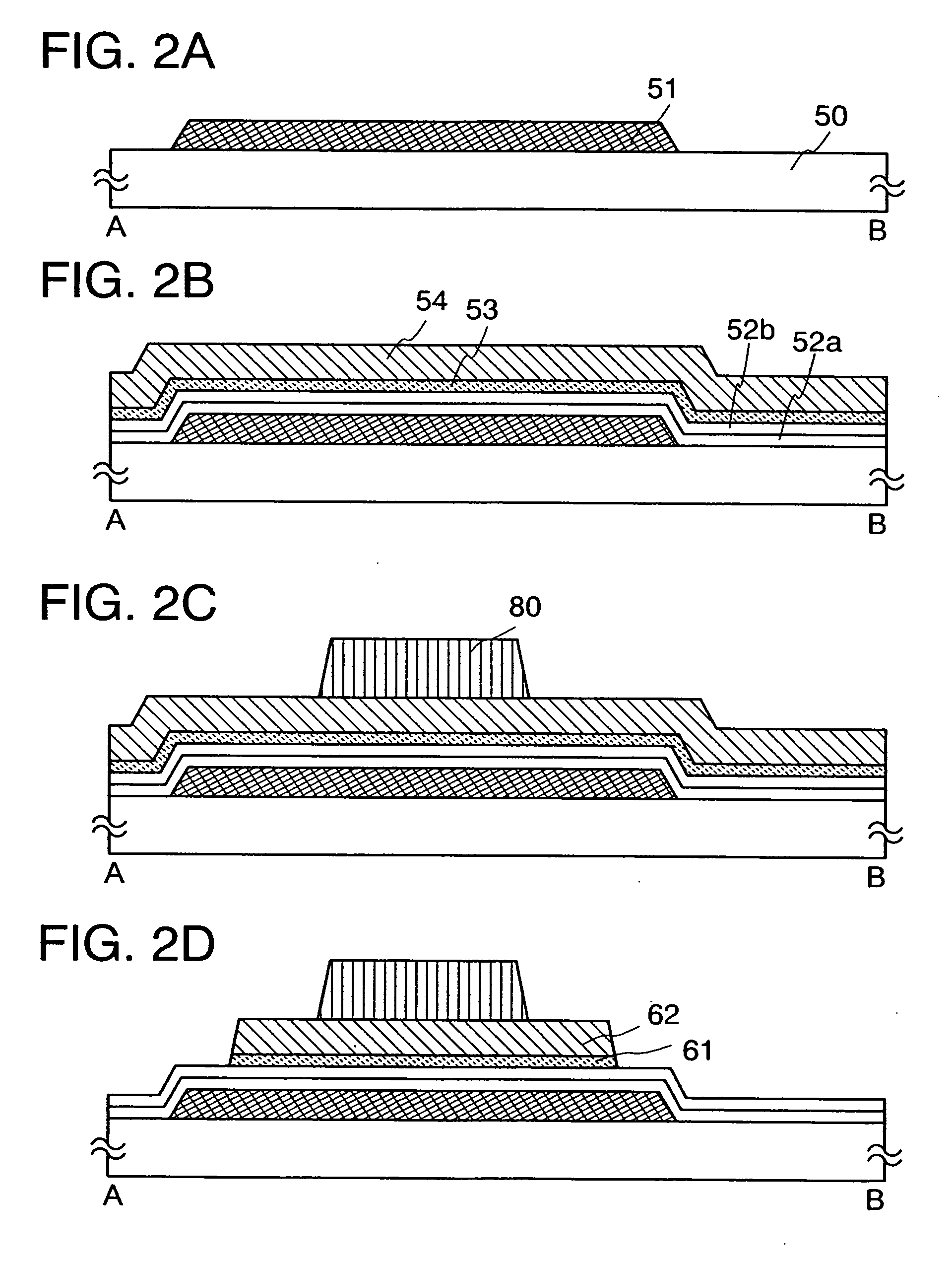
[0042]This embodiment mode will describe a thin film transistor which is used for a light-emitting device and a manufacturing process of the thin film transistor with reference to FIG. 1, FIGS. 2A to 2D, FIGS. 3A to 3C, and FIGS. 4A to 4D. FIG. 1, FIGS. 2A to 2D, and FIGS. 3A to 3C are cross-sectional views showing a thin film transistor and a manufacturing process thereof, and FIGS. 4A to 4D are plane views showing a region in a pixel where the thin film transistor and a pixel electrode are connected to each other. FIG. 1, FIGS. 2A to 2D, and FIGS. 3A to 3C are cross-sectional views showing the thin film transistor in a cross section taken along a line A-B in FIGS. 4A to 4D, and a manufacturing process thereof.
[0043]As for a thin film transistor including a microcrystalline semiconductor film, an n-type thin film transistor has higher mobility than a p-type thin film transistor; thus, an n-type thin film transistor is more suitable for a driver circuit. However, in the present inve...
embodiment mode 2
[0099]This embodiment mode will describe an example of a thin film transistor whose shape is different from that of Embodiment Mode 1. Except the shape, the thin film transistor can be formed in a similar manner to Embodiment Mode 1; thus, repetitive description of the same components or components having similar functions as in Embodiment Mode 1 and manufacturing steps for forming those components will be omitted.
[0100]This embodiment mode will describe a thin film transistor which is used for a light-emitting device and a manufacturing process of the thin film transistor with reference to FIG. 5, FIGS. 6A to 6D, and FIG. 15. FIG. 5 and FIG. 15 are cross-sectional views showing a thin film transistor and a pixel electrode, and FIGS. 6A to 6D are plane views showing a region in a pixel where the thin film transistor and the pixel electrode are connected to each other. FIG. 5 and FIG. 15 are cross-sectional views showing the thin film transistor in a cross section taken along a line ...
embodiment mode 3
[0110]This embodiment mode will describe an example of a manufacturing process in which a microcrystalline semiconductor film is irradiated with a laser beam.
[0111]A gate electrode is formed over a substrate, and a gate insulating film is formed so as to cover the gate electrode. Then, a microcrystalline silicon (SAS) film is formed as a microcrystalline semiconductor film over the gate insulating film. The thickness of the microcrystalline semiconductor film is greater than or equal to 1 nm and less than 15 nm, preferably 2 nm to 10 nm, inclusive. In particular, the microcrystalline semiconductor film with a thickness of 5 nm (4 nm to 8 nm) has high absorptance of a laser beam and improves productivity.
[0112]In the case where the microcrystalline semiconductor film is formed over the gate insulating film by a plasma CVD method or the like, near the interface between the gate insulating film and a semiconductor film which contains crystals, a region which contains more amorphous com...
PUM
 Abstract
Description
Claims
Application Information