

Radio frequency IC device and electronic apparatus
a radio frequency ic device and electronic device technology, applied in the direction of high frequency circuit adaptations, instruments, antenna earthings, etc., can solve the problems of increasing the number of manufacturing processes required to produce the rfid tag, increasing the manufacturing cost and the size of the rfid tag, and achieve the effect of easy impedance matching
- Summary
- Abstract
- Description
- Claims
- Application Information
AI Technical Summary
Benefits of technology
Problems solved by technology
Method used
Image

Examples
first preferred embodiment
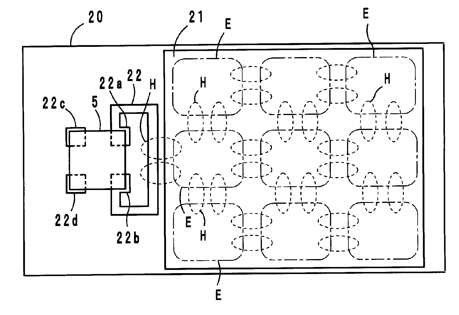
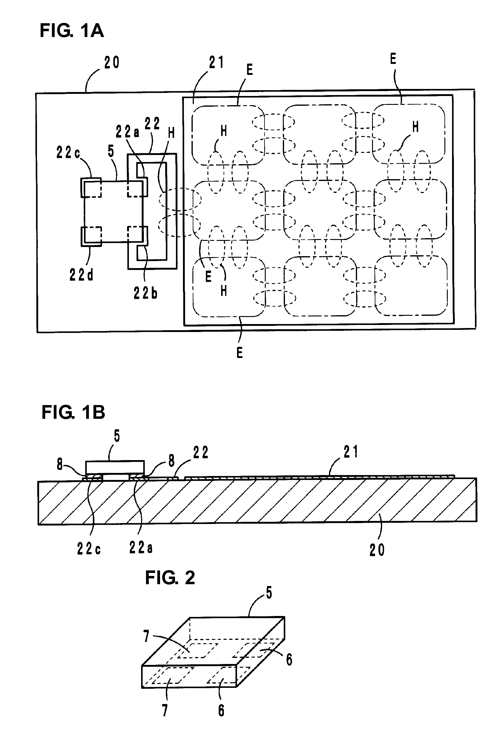
[0044]FIGS. 1A and 1B are diagrams illustrating a radio frequency IC device according to the first preferred embodiment of the present invention. This radio frequency IC device includes a radio frequency IC chip 5 arranged to process a transmitted / received signal of a predetermined frequency, a printed circuit board 20 on which the radio frequency IC chip 5 is mounted, and a ground electrode 21 and a loop electrode 22 which are arranged on the printed circuit board 20. Each of the ground electrode 21 and the loop electrode 22 is formed on the main surface of the printed circuit board 20 preferably by applying coating of conductive paste thereto or by etching metal foil on the printed circuit board 20.
[0045]The radio frequency IC chip 5 includes a clock circuit, a logic circuit, and a memory circuit, and stores necessary information. As illustrated in FIG. 2, input-output terminal electrodes 6 and mounting terminal electrodes 7 are provided on the undersurface of the radio frequency ...
second preferred embodiment
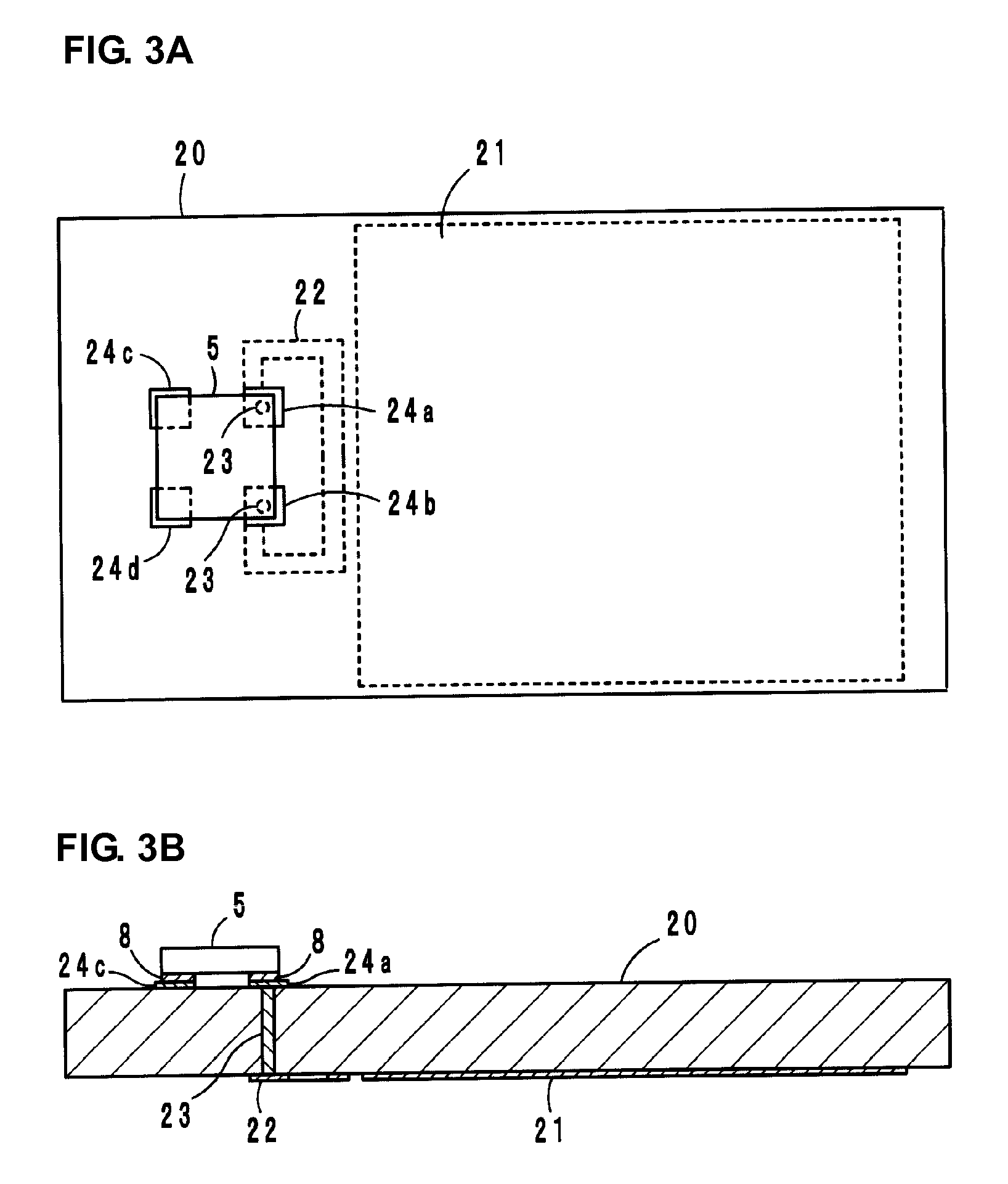
[0050]FIGS. 3A and 3B are diagrams illustrating a radio frequency IC device according to the second preferred embodiment of the present invention. This radio frequency IC device is substantially the same as a radio frequency IC device according to the first preferred embodiment. The ground electrode 21 and the loop electrode 22 are disposed on the bottom surface of the printed circuit board 20. Connection electrodes 24a to 24d are provided on the surface of the printed circuit board 20. The connection electrodes 24a and 24b are electrically connected through a via-hole conductor 23 to one end of the loop electrode 22 and the other end of the loop electrode 22, respectively. The connection electrodes 24a to 24d correspond to the connection electrodes 22a to 22d illustrated in FIGS. 1A and 1B. One of the input-output terminal electrodes 6 (see FIG. 2) is preferably electrically connected to the connection electrode 24a via the metal bump 8, for example, and the other one of the input-...
third preferred embodiment
[0052]FIGS. 4A to 4C are diagrams illustrating a radio frequency IC device according to the third preferred embodiment of the present invention. In this radio frequency IC device, a loop electrode 25 includes connection electrodes 25a and 25b disposed on the surface of the printed circuit board 20, via-hole conductors 28, and an internal electrode 29. The loop electrode 25 is coupled to the ground electrode 21 disposed on the bottom surface of the printed circuit board 20 by electric field coupling. The connection electrodes 25a and 25b are preferably electrically connected via the metal bump 8 to the terminal electrodes 6 (see, FIG. 2). Connection electrodes 25c and 25d are electrically connected via the metal bump 8 to the terminal electrodes 7 (see, FIG. 2).
[0053]The loop electrode 25 is arranged near the ground electrode 21 in the vertical direction, and is coupled to the ground electrode 21 by electric field coupling. That is, a magnetic flux is generated from the loop electrod...
PUM
 Abstract
Description
Claims
Application Information