Solid-state photosensor with electronic aperture control

Inactive Publication Date: 2009-01-29
CSEM CENT SUISSE DELECTRONIQUE & DE MICROTECHNIQUE SA RECH & DEV
View PDF9 Cites 14 Cited by
  • Summary
  • Abstract
  • Description
  • Claims
  • Application Information

AI Technical Summary

Benefits of technology

[0025]The photosensor with electronic aperture control according to the invention overcomes the disadvantages of the prior art in several respects. The effective geometric aperture of all pixels of an image detector can be changed with electrical signals, directly on the pixel level in the semiconductor domain, withou

Problems solved by technology

None of these electrically controllable optical attenuators can be implemented monolithically in the image sensor itself.
The two major disadvantages of this technique are on one hand the charge or voltage noise contributed by the channels of the multiplying transistors, and on the other hand the low operati

Method used


Image

  • Solid-state photosensor with electronic aperture control
  • Solid-state photosensor with electronic aperture control
  • Solid-state photosensor with electronic aperture control

Examples


Example

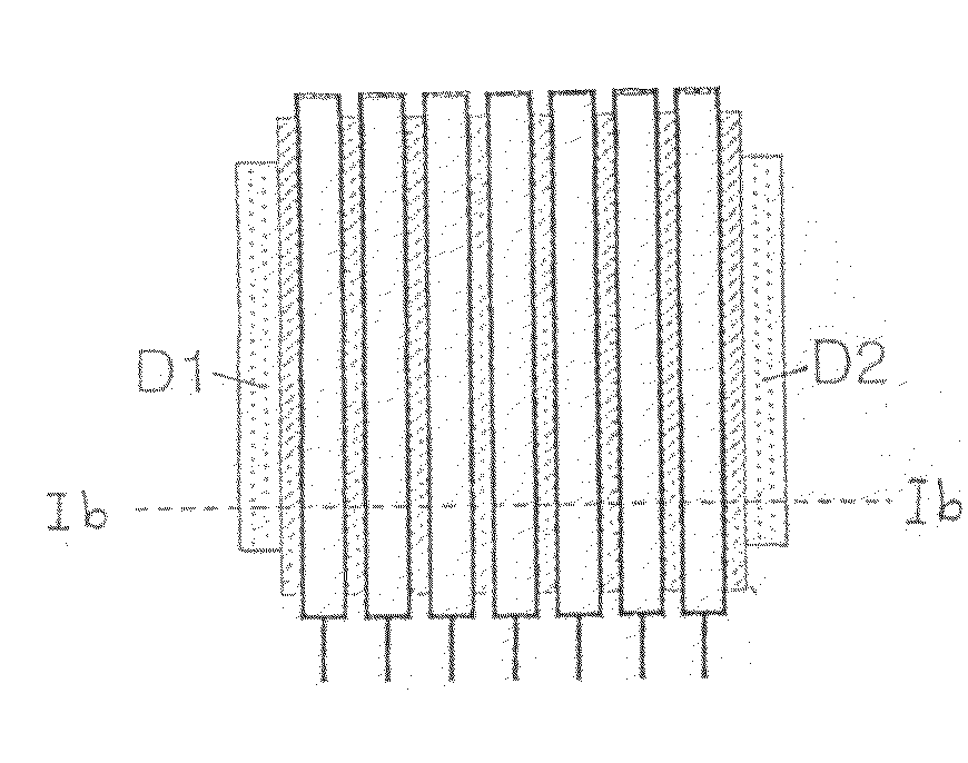
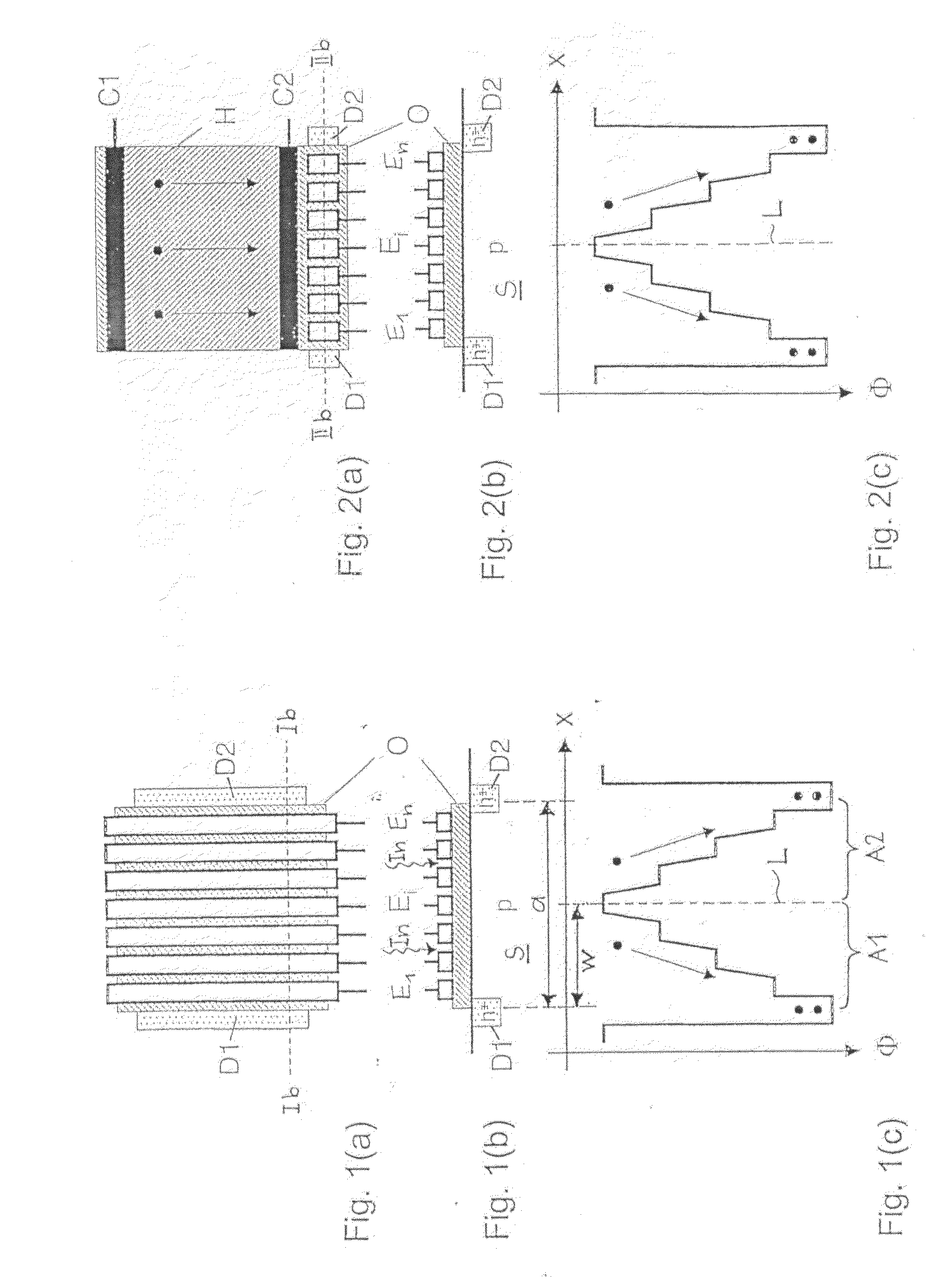
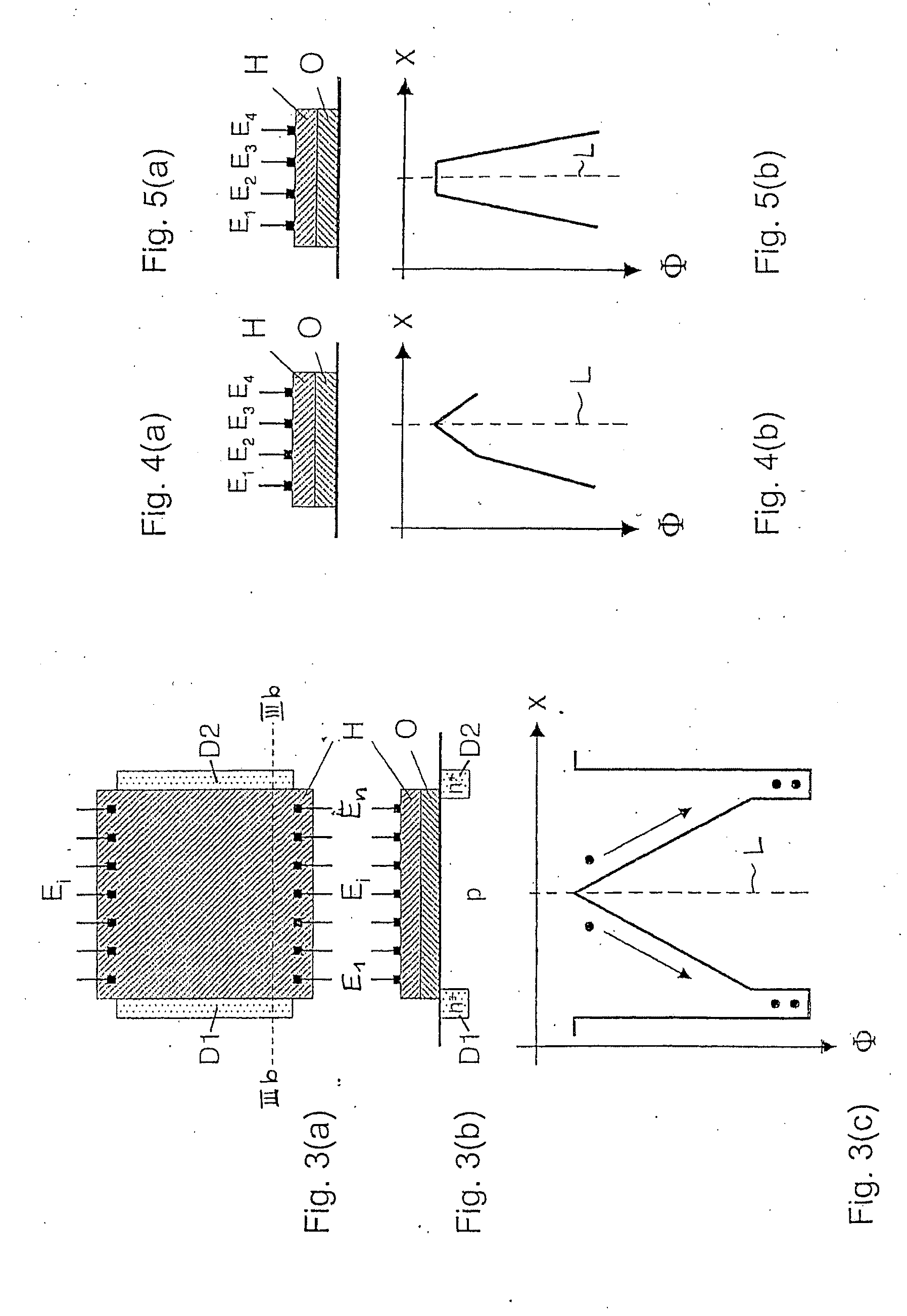
[0030]A first embodiment of the photosensor according to the invention is shown in FIG. 1(a) in a top view and in FIG. 1(b) in a cross section. The photosensor makes use of a substrate S made of a semiconductor material such as silicon for the conversion of incident photons into electron-hole pairs. Without loss of generality, we can assume in the following that this semiconductor substrate material is p-doped, and that we want to detect photoelectrons as minority charge carriers in the semiconductor material. All subsequent arguments can be suitably modified to hold true for the detection of photogenerated holes as minority carriers in n-doped semiconductor material.

[0031]The semiconductor substrate S is covered with a preferably transparent insulator layer O, preferably an oxide, as available in industry standard CMOS processes. The thickness of the insulator layer O may vary between 1 nm and 1 μm. Thinner insulator layers O let a larger part of electric surface fields pass throug...


PUM


Abstract

The effective photosensitive area of a solid-state photosensor is controlled with a multitude of electrodes (E1, . . . , Ei, . . . , En) on top of an insulator layer (O) covering a semiconductor substrate (S). Photogenerated charge carriers move laterally under the influence of the voltage distribution on the various electrodes (E1, . . . , Ei, . . . , En), and they are collected at the two ends of the photosensor in diffusions (D1, D2). The voltage distribution on the electrodes (E1, . . . , Ei, . . . , En) is such that the voltage at the two furthermost electrodes (E1, En) is maximum (if photoelectrons are collected), minimum at an interior electrode (Ei), and monotonously decreasing in between. The lateral position of the electrode (Ei) with minimum voltage defines the effective photosensitive area of the photosensor. This photosensor can be used as pixel device in image sensors, either for dynamic exposure control, for optoelectronic mixing or for demodulation, such as required in optical time-of-flight range cameras.

Description

FIELD OF THE INVENTION[0001]The present invention relates to all sensing and measuring techniques that require electrical control over the effective photosensitive area in a solid-state device that is sensitive to quasi-static or temporally modulated electromagnetic wavefields, preferably in the ultraviolet, visible or infrared spectral range. When used quasi-statically, this capability is required for the dynamic control of the sensitivity of the photosensor, to replace or enhance the function of a shutter. In this way, the dynamic range of the photosensor is improved and can be adapted to the lighting conditions in a scene. When used at high frequency, this capability is required for the mixing of incident modulated light with an analog time-function, or for the demodulation of the incident light, as needed in particular for non-contact distance measurement techniques based on optical phase-shifting interferometry or on time-of-flight ranging. The present invention relates specifi...

Claims


Application Information

Patent Timeline
IPC IPC(8): H01L27/146H04N5/335
CPCH01L27/146H01L31/113H01L27/148
Inventor SEITZ, PETER
Owner CSEM CENT SUISSE DELECTRONIQUE & DE MICROTECHNIQUE SA RECH & DEV
Why Eureka
Try Eureka