Stacked electronic part and method of manufacturing the same

a technology of electronic parts and stacked components, which is applied in the direction of stacked capacitors, positive temperature coefficient thermistors, resistor details, etc., can solve the problem that the deposition of a ceramic green body plating cannot be sufficiently suppressed, and achieve the effect of reducing the ratio of occurrence (frequency) of “bursting and positively preventing corrosion of the external electrode by the plating liquid

Active Publication Date: 2009-01-29
TDK CORPARATION
View PDF3 Cites 24 Cited by
  • Summary
  • Abstract
  • Description
  • Claims
  • Application Information

AI Technical Summary

Benefits of technology

[0013]In contrast to this, it was ascertained that in a stacked electronic part of the present invention, the occurrence of such “bursting” can be effectively suppressed and it became apparent that in particular, when the resin filling ratio in a porous green body is not less than 80%, it is possible to substantially reduce the ratio of occurrence (frequency) of “bursting.”
[0014]The present invention is more useful when the porous green body is a burned body (a sintered compact) and its sintered density (measured density / theoretical density×100%) is not less than 90%. That is, according to the studies conducted by the present inventors, it was ascertained that plating deposition on the surface of a porous green body is scarcely observed during the forming of a terminal electrode when the porous green body having a sintered density exceeding 90% is used, whereas the rate of plating deposition on the surface of the porous green body increases abruptly as the sintered density decreases. It might be thought that this is because open pores scarcely occur when the sintered density of a porous green body exceeds 90% and even when vacancies are generated, most of them are closed pores and the plating liquid does not enter, whereas the total number of open pores and the ratio of open pores to all vacancies increases abruptly when the sintered density becomes not more than 90%. Therefore, the operation and effect of the present invention are more advantageously realized when the present invention is applied to a stacked electronic part having a porous green body with a sintered density of not more than 90%, in which such a large number of open pores can be formed.
[0015]When a stacked electronic part of the present invention further includes an overcoat layer that covers the external electrode, the corrosion of the external electrode by the plating liquid can be positively prevented when a terminal electrode is formed on the surface of the external electrode by plating.
[0016]Furthermore, a method of manufacturing a stacked electronic part according to the present invention, which is a method for effectively manufacturing the stacked electronic part of the present invention, comprises the steps of: forming a stacked structure by providing at least one internal electrode within a porous green body made mainly of ceramics and containing a plurality of vacancies; forming a stacked body (a sintered compact) by burning (sintering) the stacked structure; applying an electrically conductive paste to the stacked body so as to obtain an electrical connection to the internal electrode of the stacked body; forming an external electrode by burning (sintering) the electrically conductive paste; filling resin in the plurality of vacancies at a filling ratio of not less than 60%, preferably not less than 70%, most preferably not less than 80% by impregnating resin in the porous green body; and forming a terminal electrode on the external electrode by plating.

Problems solved by technology

In contrast to this, when the whole surface of a ceramic green body was impregnated with a silicone resin by using a conventional method disclosed in Japanese Patent No. 2700978, it was ascertained that under some resin impregnation conditions, the deposition of a plating on the ceramic green body cannot be sufficiently suppressed.

Method used


Image

  • Stacked electronic part and method of manufacturing the same
  • Stacked electronic part and method of manufacturing the same
  • Stacked electronic part and method of manufacturing the same

Examples


first embodiment

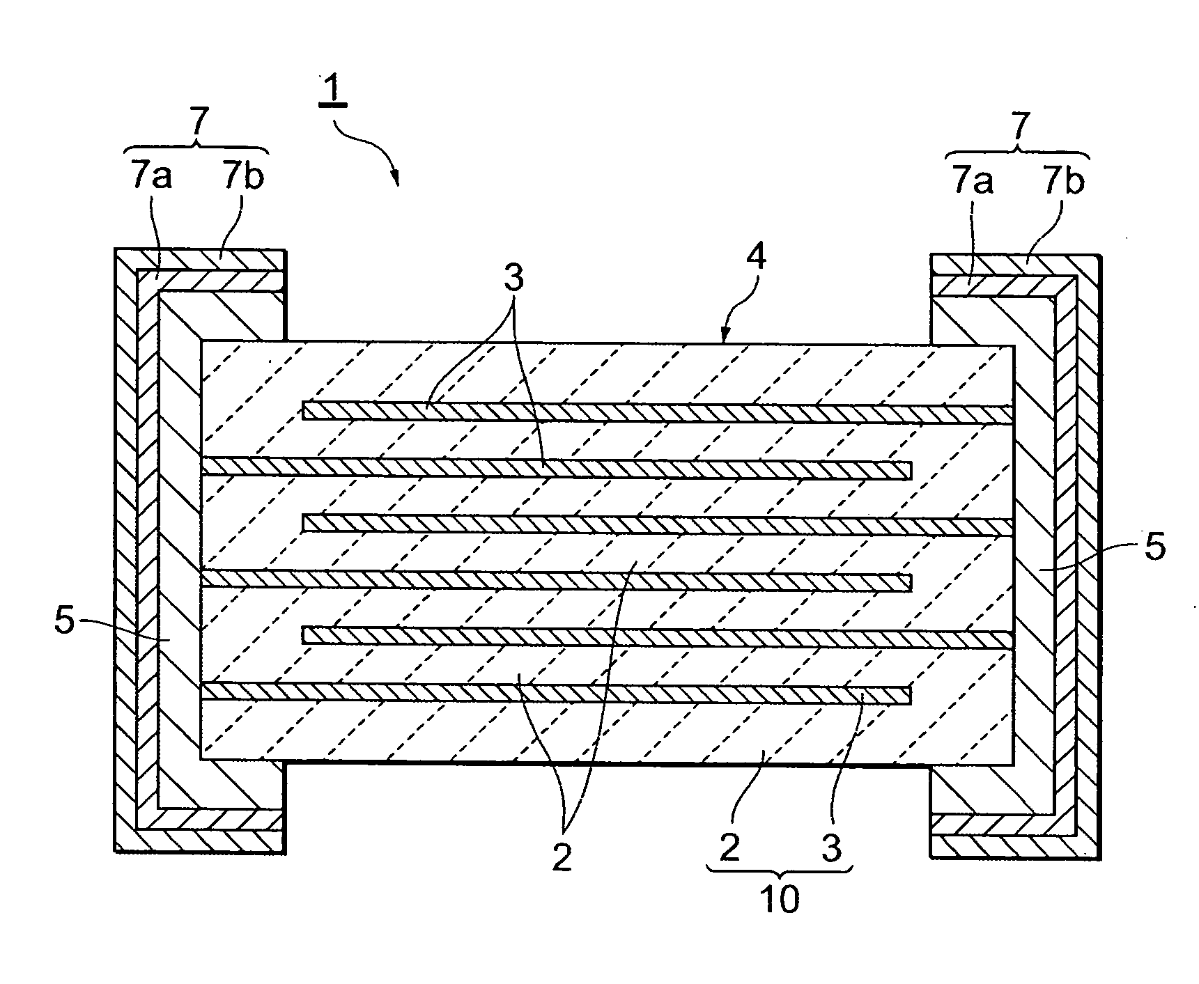
[0040]FIG. 1 is a sectional view showing the schematic construction of the first embodiment of a stacked electronic part according to the present invention. The stacked electronic part 1 is a PTC thermistor having a stacked body 4 that includes a porous green body 2 made mainly of ceramics and containing a plurality of vacancies and a plurality of internal electrodes 3 formed within the porous green body 2. In other words, the stacked electronic part 1 is provided with at least one unit structure 10 in which the porous green body 2 and the internal electrodes 3 are stacked. More concretely, an internal electrode 3 having an end portion exposed to one side surface of the stacked body 4 and an internal electrode 3 having an end portion exposed to the other side surface of the stacked body 4 are alternately stacked.

[0041]On both side surfaces of the stacked body 4, there are provided external electrodes 5, 5 so as to cover these side surfaces, and each of the external electrodes 5 is e...

second embodiment

[0069]FIG. 8 is a sectional view showing the schematic construction of the second embodiment of a stacked electronic part according to the present invention. A stacked electronic part 9 is constructed in the same manner as the stacked electronic part shown in FIG. 1, with the exception that an overcoat layer 8 containing Ag as a metal component is formed so as to cover an external electrode 5. This overcoat layer 8 can be formed by printing and burning an electrically conductive paste containing, for example, Ag. Incidentally, though not illustrated, in FIG. 8, terminal electrodes 7, 7 are formed in a stacked manner on the outer side of the overcoat layers 8, 8.

[0070]According to the stacked electronic part 9 of this construction, because of the formation of the overcoat layer 8 on the surface of the external electrode 5, it is possible to more positively prevent the Al and the like that are contained in the external electrode 5 from being corroded by the plating liquid for forming ...

examples 1 to 5

[0074]By changing the resin filling ratio of the porous green body 2 whose sintered density is 80%, a plurality of five kinds of PTC thermistors each having a resin filling ratio of not less than 60% according to the present invention were manufactured by following the above-described procedure for manufacturing PTC thermistors. Incidentally, impregnation was performed once or repeated a plurality of times, and the resin filling ratio was appropriately adjusted by the times of number of impregnation.


PUM

PropertyMeasurementUnit
densityaaaaaaaaaa
electrically conductiveaaaaaaaaaa
electrical propertiesaaaaaaaaaa

Abstract

Provided are a stacked electronic part that can sufficiently suppress plating deposition on the surface of a porous green body when a terminal electrode is formed on an external electrode, thereby enabling a decrease in the reliability of products to be prevented, and a method of manufacturing the stacked electronic part. The stacked electronic part 1 is a PTC thermistor having a stacked body 4 containing a porous green body 2 made of ceramics and having a plurality of vacancies and a plurality of internal electrodes 3 formed within the porous green body 2, and is provided with at least one unit structure 10 in which the porous green body 2 and the internal electrode 3 are stacked. External electrodes 5, 5 are connected to the internal electrode 2, and upon the external electrodes 5, 5 are formed terminal electrodes 7, 7 by plating. Resin is filled in the plurality of vacancies of the porous green body 2 at a filling ratio of not less than 60%.

Description

BACKGROUND OF THE INVENTION[0001]The present invention relates to a stacked electronic part having a stacked structure provided with a green body made of ceramics and an internal electrode and a method of manufacturing the stacked electronic part.[0002]In general, a stacked electronic part formed from a thermistor, a capacitor, an inductor, LTCC (Low Temperature Co-fired Ceramics) and a varistor that has a ceramic green body, an internal electrode and an external electrode, and from a complex thereof is mounted on a wiring board, such as a printed circuit board, and the external electrode is soldered in a prescribed connection point. On that occasion, if an terminal electrode composed of an Ni layer and an Sn layer is formed, by plating, on an external electrode (a front-end electrode) made of, for example, Ag, is used, the bonding properties of a solder to the substrate are improved and productivity can be improved.[0003]In order to prevent the worsening of the electrical propertie...

Claims


Application Information

Patent Timeline
Patent Type & Authority Applications(United States)
IPC IPC(8): H01C7/02H01C17/00
CPCH01C1/14Y10T29/49085Y10T29/49082H01C7/02H01G4/30
Inventor KAJINO, TAKASHIABE, HISAYUKIKAKINUMA, AKIRAITOH, KAZUHIKO
Owner TDK CORPARATION
Why Eureka
Try Eureka