TFT LCD array substrate and method of manufacturing thereof
a technology of array substrate and pixel electrode, which is applied in the direction of optics, semiconductor devices, instruments, etc., can solve the problems of serious restrictions on the charging and discharging of pixel electrodes, degraded display quality, and uneven color distribution over the whole screen, so as to improve the yield of products and enhance the display quality of products
- Summary
- Abstract
- Description
- Claims
- Application Information
AI Technical Summary
Benefits of technology
Problems solved by technology
Method used
Image
Examples
first embodiment
The First Embodiment
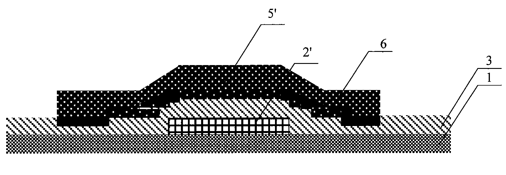
[0025]FIG. 1 is a schematic view of an array substrate having an air gap according to an embodiment of the invention. As shown in FIG. 1, a TFT LCD array substrate comprises a substrate 1, a gate scanning line 2′ and a signal scanning line 7 formed on the substrate 1 and intersecting each other to define a pixel unit, an insulating layer 3 and an active layer 5 formed between the gate scanning line 2′ and the signal scanning line 7, and an air gap 6 provided between the insulating layer 3 and the active layer 5 at the position where the gate scanning line and the signal scanning line intersect each other.
[0026]On the substrate 1, there are formed the gate scanning line 2′, the insulating layer 3, the air gap 6, the active layer 5′, and the signal scanning line 7 in order. The formed air gap 6 has the same wideness in the direction of the gate scanning line 2′ as that of the active layer 5, and has the same wideness in the direction of the signal scanning line 7 a...
second embodiment
The Second Embodiment
[0035]As shown in FIG. 8, the embodiment according to the invention provides a method for manufacturing an array substrate having an air gap. The method comprises the following steps of:
[0036]step 1, a metal film is deposited and patterned on a substrate, and a gate scanning line is formed by lithography process and etching process;
[0037]step 2, an insulating layer is deposited on the substrate;
[0038]step 3, a photoresist layer is applied and patterned on the insulating layer on the substrate, and the photoresist is remained at the intersection of the gate scanning line and a signal scanning line, which is to be formed subsequently, after lithography process and etching process;
[0039]step 4, an active covering layer is deposited and patterned on the substrate by the lithography and etching process so that there are formed an active layer of a thin film transistor and an active layer partially covering the remained photoresist in a direction of the gate scanning ...
PUM
| Property | Measurement | Unit |
|---|---|---|
| width | aaaaa | aaaaa |
| volume | aaaaa | aaaaa |
| area | aaaaa | aaaaa |
Abstract
Description
Claims
Application Information
 - R&D
- Intellectual Property
- Life Sciences
- Materials
- Tech Scout
- Unparalleled Data Quality
- Higher Quality Content
- 60% Fewer Hallucinations
Browse by: Latest US Patents, China's latest patents, Technical Efficacy Thesaurus, Application Domain, Technology Topic, Popular Technical Reports.
© 2025 PatSnap. All rights reserved.Legal|Privacy policy|Modern Slavery Act Transparency Statement|Sitemap|About US| Contact US: help@patsnap.com


