

Semiconductor device and electrical circuit device using thereof
a technology of semiconductor devices and circuit devices, applied in the direction of semiconductor devices, basic electric elements, electrical apparatus, etc., can solve the problems of large electrical field generated on the oxide film, low reliability, etc., and achieve the effect of low threshold voltage and large saturation curren
- Summary
- Abstract
- Description
- Claims
- Application Information
AI Technical Summary
Benefits of technology
Problems solved by technology
Method used
Image

Examples
first embodiment
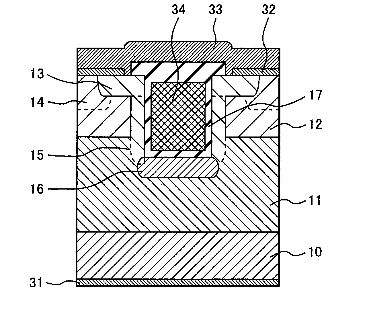
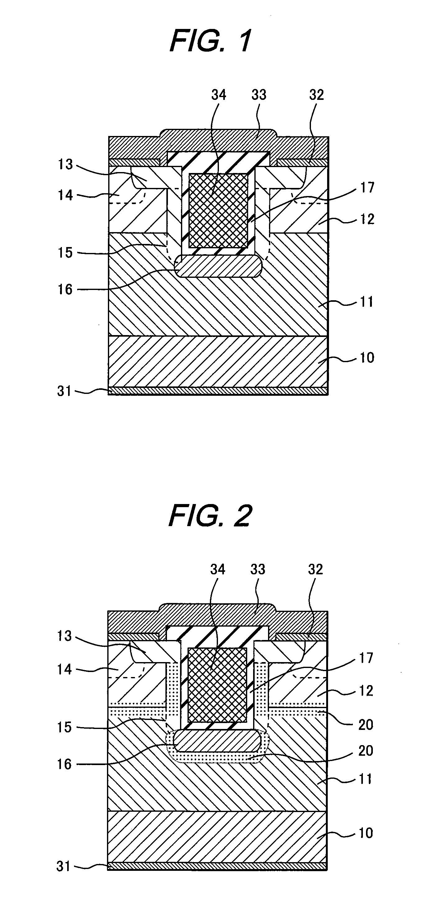
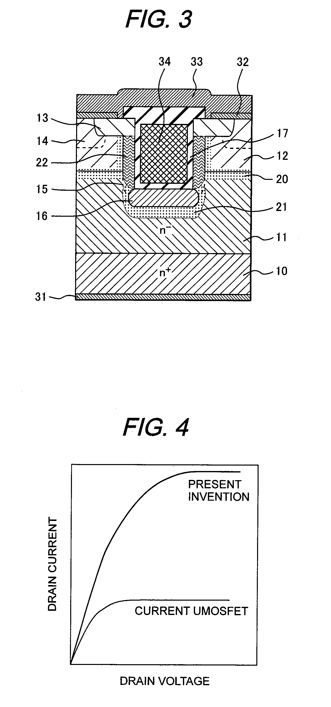
[0045]FIG. 1 is a cross sectional view of a UMOSFET according to a first embodiment of the present invention. FIGS. 5 to 12 are diagrams showing an outline process for forming the UMOSFET according to the first embodiment.
[0046]As shown in FIG. 5, the N− type SiC drift layer 11 (having an impurity concentration of 2×1016 cm−3 and a thickness of 6.5 μm) is provided on the N+ type SiC wafer 10. The P type body 12 (having an impurity concentration of 1×1018 cm−3 and a thickness of 2.3 μm) is provided on the drift layer 11. The drift layer 11 and the P type body 12 are semiconductor layers. A first mask material 40 for ion implantation is provided on the P type body 12. The first mask material 40 is patterned. Nitrogen ions 41 are implanted into the structure shown in FIG. 5 to form the N+ type SiC source layer 13 (having a peak impurity concentration of 1×1020 cm−3 and a thickness of 0.3 μm). In the process, an SiO2 film formed by a chemical vapor deposition (CVD) method is used as the...
second embodiment
[0061]A circuit and a module, which use the semiconductor device according to the present invention, will be described in a second embodiment of the present invention. FIG. 16 is a diagram showing a circuit using the semiconductor device according to the present invention. The circuit shown in FIG. 16 is a three phase circuit. In FIG. 16, three phases of the circuit, which include outputs 1, 2 and 3, are juxtaposed to each other. FIG. 17 is a diagram showing the configuration of a 6-in-1 module corresponding to the circuit shown in FIG. 16. In FIGS. 16 and 17, the same reference numerals indicate the same members. Reference numeral 61 denotes a base; 50, a UMOSFET according to the present invention; 51, a P-side terminal extractor; 52, an N-side terminal extractor; 53, a P-side gate extractor; 54, an N-side gate extractor; 55, a P-side output extractor; 56, an N-side output extractor; 57, a P-side substrate; 58, an N-side substrate; and 59, a free wheel diode for back flow. FIGS. 16...
third embodiment
[0064]FIG. 18 is a cross sectional view of a SiC-IGBT, which is the semiconductor device according to a third embodiment of the present invention. In FIG. 18, reference numeral 60 denotes a P type SiC wafer; 61, an N type base layer; and 63, an N type emitter layer. In the present embodiment, the present invention is applied to a trench type IGBT. The IGBT is a bipolar transistor in which a MOSFET is embedded in a gate section. The gate section has a similar configuration to that used in the abovementioned embodiments. In the IGBT, a P type body 12 is provided on the N type base layer 61. The N type emitter layer 63 is provided in a portion of the P type body 12. A gate oxide film 17 is provided in a trench. A gate electrode 34 is provided on an inner side of the gate oxide film 17. Reference numeral 14 denotes a P+ type region. The N type emitter layer 63 is connected to an emitter electrode 73 through a silicide layer 72. Reference numeral 15 denotes a channel region. A P type ele...
PUM
 Abstract
Description
Claims
Application Information