Semiconductor device

a technology of semiconductor devices and diodes, applied in the direction of semiconductor devices, basic electric elements, electrical equipment, etc., can solve the problems of reducing dimensional to a package size, increasing the cost of connecting diodes, etc., and achieves the improvement of drain current, channel width, and saturation drain current.

Inactive Publication Date: 2007-11-01
HITACHI LTD
View PDF3 Cites 19 Cited by
  • Summary
  • Abstract
  • Description
  • Claims
  • Application Information

AI Technical Summary

Benefits of technology

[0011]FIGS. 2A and 2B are diagrams showing a spread of a depletion region DP in the JFET of the present invention. FIG. 2A shows an “off” state, and FIG. 2B shows an “on” state. Since the JFET employs trenched construction, a depletion region from a p+ emitter 16 and a depletion layer from a p+ type gate region 15 each come to overlap on the other efficiently. Accordingly, the “off” state shown in FIG. 2A can be realized at a low gate bias volta

Problems solved by technology

In the inverter, therefore, a fly-wheeling diode for the current needs to be connected in antiparallel to each JFET, so the connection

Method used


Image

  • Semiconductor device
  • Semiconductor device
  • Semiconductor device

Examples


first embodiment

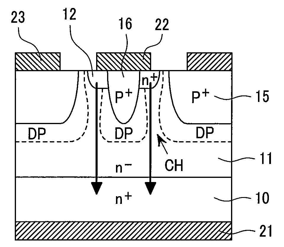
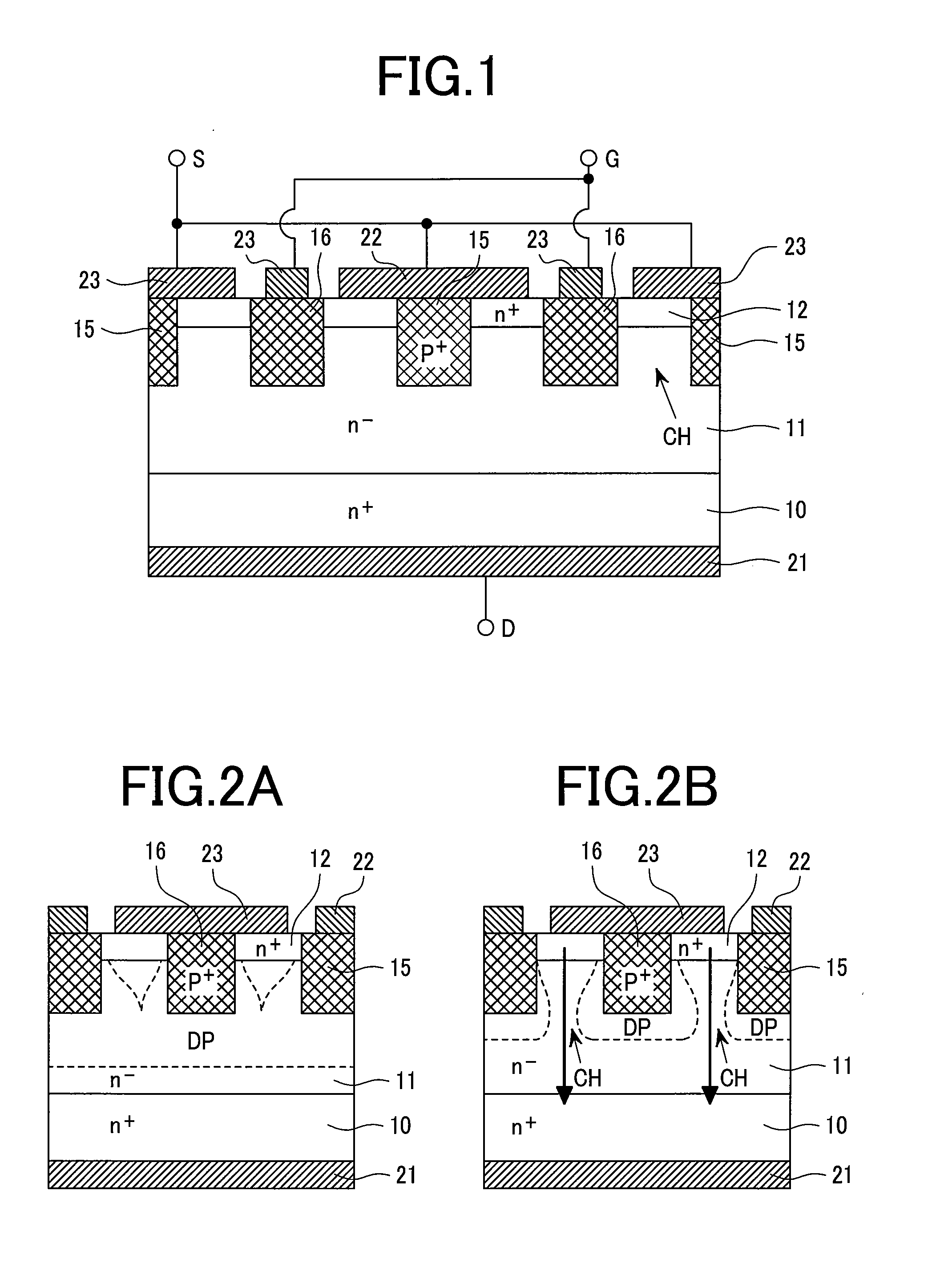
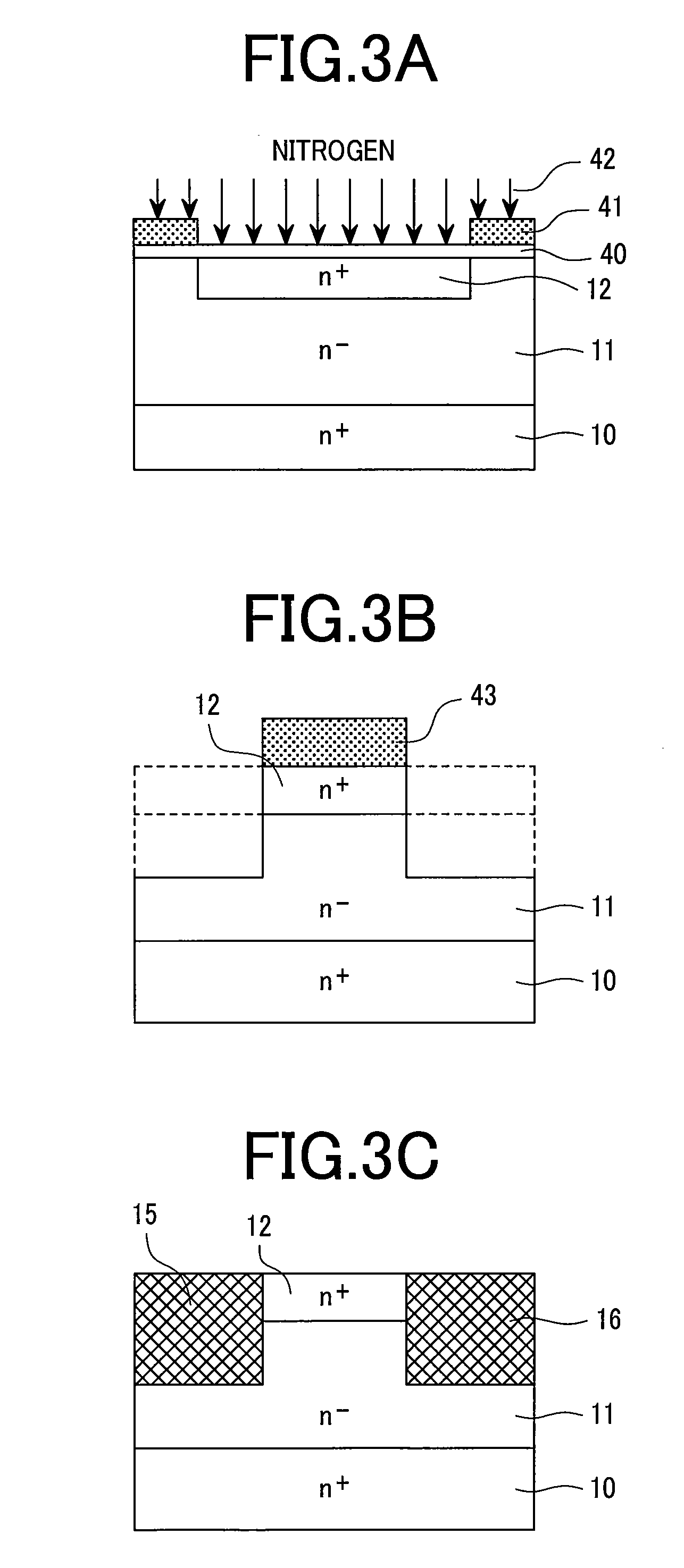
[0031]FIG. 1 is a cross-sectional view of a JFET, showing a first embodiment of a semiconductor device according to the present invention. In the first embodiment, construction that includes trench grooves filled with p-type polycrystalline silicon (hereinafter, referred to p-type poly-Si) is employed for a p+ gate region 15 and a p+ emitter region 16. FIGS. 3A to 3F are cross-sectional structural view schematically showing the process steps of forming the JFET of the first embodiment. These process steps are described in order below.

[0032]As shown in FIG. 3A, on an n+ SiC substrate 10 is first formed an n− SiC drift layer 11 (2×1016 cm−2 in concentration and 6.5 μm in thickness), on which is then formed an oxide film 40, and on which is further formed an ion implantation mask material 41. Next, the ion implantation mask material 41 on the oxide film 40 is patterned and nitrogen ions 42 are implanted to form an n+ SiC source 12 (1×1020 cm−2 in peak concentration and 0.25 μm in thick...

second embodiment

[0041]FIG. 4 is a cross-sectional structural view of a JFET, showing a second embodiment of a semiconductor device according to the present invention. The first embodiment uses the p-type poly-Si of the same concentration to fill in the entire trench. To prevent malfunctioning during switching, it is desirable that even in a normally-off state, a negative voltage be capable of being applied to the gate, and reliability of the source-gate withstand voltage needs to be guaranteed. In the present (second) embodiment, therefore, sidewalls of a channel that come into contact with an n+ source 12 of a poly-Si filler are formed as low-concentration sections 152, 162 (concentration: 2×1017 cm−3), and bottom sections of the channel, as high-concentration sections 151, 161 (concentration: 5×1019 cm−3).

[0042]This makes it possible to ensure a desired source-gate withstand voltage and to improve “off” performance. However, since direct contact of an electrode to the low-concentration poly-Si 16...

third embodiment

[0043]FIG. 5 is a cross-sectional structural view of a JFET, showing a third embodiment of a semiconductor device according to the present invention. To realize a high withstand voltage with a pn junction formed up of p-type poly-Si 163, 153 and n-type SiC, the poly-Si requires a concentration from a level slightly below 1020 cm−3 to an order of 1020 cm−3. In this context, the present embodiment is constructed to achieve a high withstand voltage at a poly-Si concentration of an order of 1018 cm−3, and has a p-type SiC layer 17, 18 at bottom sections of trenches and at sidewalls of each trench. The p-type SiC layers 17, 18 are 1×1018 cm−3 in concentration and 0.2 μm in thickness. The trenches in this case are 1.0 μm spaced and have a width of 1.0 μm and a depth of 1.3 μm. This trench structure renders a high withstand voltage of 750 V achievable without generating a high electric field in the poly-Si 163, since a depletion layer from a drain side of an n− drift layer 11 stays inside ...


PUM


Abstract

The present invention can maintain a blocking state, even at a low gate bias voltage, in a diode-containing type of junction FET, and achieves a large saturation current.
The junction FET includes: an n+ SiC substrate 10 as a drain layer; an n SiC layer 11 contiguous to the drain layer as a drift layer; an n+ SiC layer 12 formed on the drift layer as a source layer; trench grooves formed ranging from the source layer to a required depth of the drift layer and part of the drift layer as a channel region; and p-type polycrystalline Si formed in the trench grooves as gate regions. The gate region at one side of the channel is electrically shorted to a source electrode to form a p emitter of a diode.

Description

CLAIM OF PRIORITY[0001]The present application claims priority from Japanese application JP 2006-121760 filed on Apr. 26, 2006, the content of which is hereby incorporated by reference into this application.BACKGROUND OF THE INVENTION[0002]1. Field of the Invention[0003]The present invention relates generally to semiconductor devices, and more particularly to a semiconductor device suitable for junction FETs (JFETs) or static induction transistors (SITs).[0004]2. Related Art[0005]In an inverter circuit constituted by JFETs or SITs, since a motor or the like is used as a load, a mode exists that causes inductance to generate a flow of a current in an inverse direction when the JFETs are off. In the inverter, therefore, a fly-wheeling diode for the current needs to be connected in antiparallel to each JFET, so the connection of the diodes correspondingly increases costs. There has also been the problem that dimensional reduction to a package size is limited.[0006]Silicon carbide (SiC)...

Claims


Application Information

Patent Timeline
IPC IPC(8): H01L31/112
CPCH01L29/0692H01L29/1608H01L29/8083H01L29/7722H01L29/66409
Inventor ONOSE, HIDEKATSU
Owner HITACHI LTD
Why Eureka
Try Eureka