Nitrogen-enhanced GaN-based Heterojunction Field-Effect Transistor with Composite Barrier Layer

A heterojunction field effect and composite barrier technology, which is applied in semiconductor devices, electrical components, circuits, etc., can solve the problems of high etching process requirements, degradation of device sub-threshold characteristics, and reduced device gate control ability, etc., to achieve Effects of avoiding defects, reducing polarization strength, and large saturation drain current

Active Publication Date: 2021-04-02
UNIV OF ELECTRONICS SCI & TECH OF CHINA
View PDF1 Cites 0 Cited by
  • Summary
  • Abstract
  • Description
  • Claims
  • Application Information

AI Technical Summary

Problems solved by technology

These two methods can effectively realize the high-threshold enhanced operation of the device, but the groove gate structure has high requirements on the etching process, and the etching damage will seriously affect the channel mobility of carriers; although the epitaxial cap layer The process is simple and controllable, and has no effect on channel mobility, but the introduction of a cap layer under the gate will inevitably reduce the gate control capability of the device, resulting in the degradation of the subthreshold characteristics of the device

Method used


Image

  • Nitrogen-enhanced GaN-based Heterojunction Field-Effect Transistor with Composite Barrier Layer
  • Nitrogen-enhanced GaN-based Heterojunction Field-Effect Transistor with Composite Barrier Layer
  • Nitrogen-enhanced GaN-based Heterojunction Field-Effect Transistor with Composite Barrier Layer

Examples


Embodiment 1

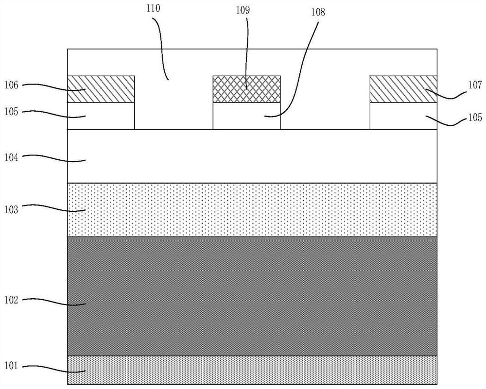
[0035] like figure 2 As shown, a nitrogen-surface-enhanced composite barrier layer gallium nitride-based heterojunction field effect transistor in this embodiment includes: a substrate 101, a gallium nitride buffer layer 102 arranged on the upper layer of the substrate 101, a nitride Gallium nitride channel layer 104, source 106, drain 107, gate 109, N+ type semiconductor layer 105, passivation layer 110, composite barrier layer above the gallium buffer layer 102, the N+ type semiconductor layer 105 is set Above the gallium nitride channel layer 104, the source electrode 106 and the drain electrode 107 are arranged above the N+ type semiconductor layer 105 and both form ohmic contacts with the N+ type semiconductor layer 105, and the gate electrode 109 is arranged on the nitride Above the gallium channel layer 104, the composite barrier layer is arranged between the gallium nitride buffer layer 102 and the gallium nitride channel layer 104, and the composite barrier layer inc...

Embodiment 2

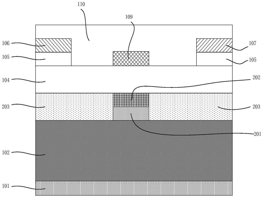
[0044] like image 3 As shown, the difference between this example and the first example is that an insulating dielectric layer 108 is disposed above the gallium nitride channel layer 104 , and the gate 109 is disposed above the insulating dielectric layer 108 .

[0045] The following will image 3 The shown nitrogen facet-enhanced GaN HFET with composite barrier layer and figure 1 The comparison of the conventional nitrogen-faced GaN HFET shown; the structural parameters of the device are given in Table 1 as an example.

[0046] Table 1 Device simulation structure parameter table

[0047] Device parameter name Conventional Nitrogen Surface GaN HFET Nitrogen surface GaN HFET of the present invention Gate length 0.62μm 0.62μm source length 0.5μm 0.5μm Gate-to-source spacing 0.05μm 0.05μm GaN buffer layer thickness 200μm 200μm barrier layer thickness 2nm 2nm GaN channel layer thickness 20nm 20nm AlGaN bar...

Embodiment 3

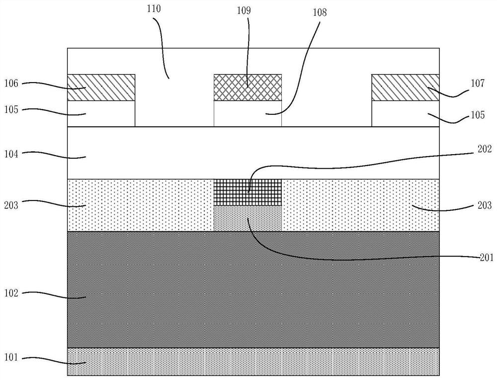
[0052] like Figure 4 As shown, the difference between this example and the second example is that the lengths of the GaN layer 201 and the AlGaN layer 202 are greater than the length of the gate 109 .

[0053] By increasing the length of the AlGaN layer and the AlN layer, the two-dimensional electron gas in the channel of the non-gate region can be further depleted. This scheme can further increase the device threshold voltage, but it will reduce The two-dimensional electron gas density of the channel leads to a decrease in the drain current when the device is turned on.


PUM

PropertyMeasurementUnit
thicknessaaaaaaaaaa
thicknessaaaaaaaaaa
thicknessaaaaaaaaaa

Abstract

The present invention provides a nitrogen surface enhanced compound barrier layer gallium nitride based heterojunction field effect transistor, comprising: a substrate, a gallium nitride buffer layer, a gallium nitride channel layer, a source, a drain, and a gate , N+ type semiconductor layer, passivation layer, composite barrier layer, the composite barrier layer includes an aluminum nitride layer, and a composite structure composed of a gallium nitride layer and an aluminum gallium nitride layer, and the gallium nitride layer is located below the aluminum gallium nitride layer , the present invention realizes the enhanced nitrogen surface gallium nitride-based heterojunction field effect transistor through the compound barrier layer structure, and reduces the barrier layer material of aluminum gallium nitride and gallium nitride under the gate, reducing the Polarization of the lower channel, thus depleting the 2D electron gas channel. When the gate voltage increases positively, the depletion region of the channel layer under the gate becomes narrower, thereby opening the two-dimensional electron gas channel. Such structures have a larger saturation drain current, while avoiding the effects of defects caused by doping.

Description

technical field [0001] The invention relates to the epitaxial structure of microelectronic devices, in particular to the field of gallium nitride heterojunction field effect transistors. Background technique [0002] Wide bandgap gallium nitride (GaN)-based heterojunction field effect transistor (HFET) is a kind of field effect transistor, the material used is a heterojunction structure, and the two-dimensional electron gas ( 2DEG) form a conductive channel. Gallium nitride heterojunction field effect transistor has the advantages of high critical breakdown electric field, fast electron saturation speed, high thermal conductivity and excellent frequency characteristics, and has become a strong candidate for the next generation of power semiconductor devices. [0003] Nitride wurtzite structure crystals have two polarities of Ga plane and N plane, and the physical and chemical properties of different polar planes show obvious differences, so the two polarities are not equiva...

Claims


Application Information

Patent Timeline
Patent Type & Authority Patents(China)
IPC IPC(8): H01L29/06H01L29/778
CPCH01L29/0684H01L29/7781
Inventor 杜江锋鲁岩杨荣森刘勇于奇
Owner UNIV OF ELECTRONICS SCI & TECH OF CHINA
Why Eureka
Try Eureka