Memory structure and manufacturing method thereof

a technology of memory structure and manufacturing method, which is applied in the direction of semiconductor devices, electrical apparatus, transistors, etc., can solve the problems of requiring a lot of energy and time to move data back and forth between various memories, and achieve the effect of improving electrical performan

Active Publication Date: 2021-04-06
POWERCHIP SEMICON MFG CORP
View PDF3 Cites 0 Cited by
  • Summary
  • Abstract
  • Description
  • Claims
  • Application Information

AI Technical Summary

Benefits of technology

[0005]The invention provides a memory structure and a manufacturing method thereof, which can have a better electrical performance.
[0026]Based on the above description, in the memory structure and the manufacturing method thereof according to the invention, since the first nickel silicide layer and the second nickel silicide layer are respectively located on the first doped region and the second doped region, the transistor in the peripheral circuit region can have lower resistance and larger saturation current. Thereby, the performance of the transistor can be effectively improved. Thus, the electrical performance of the memory structure can be improved.

Problems solved by technology

However, when performing a large amount of data processing, it requires a lot of energy and time to move data back and forth between various memories and processors.

Method used


Image

  • Memory structure and manufacturing method thereof
  • Memory structure and manufacturing method thereof
  • Memory structure and manufacturing method thereof

Examples


Embodiment Construction

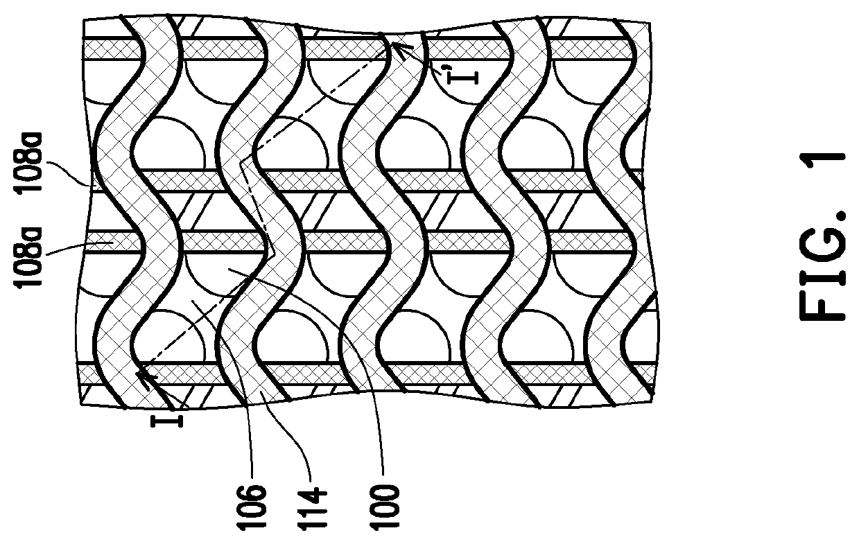
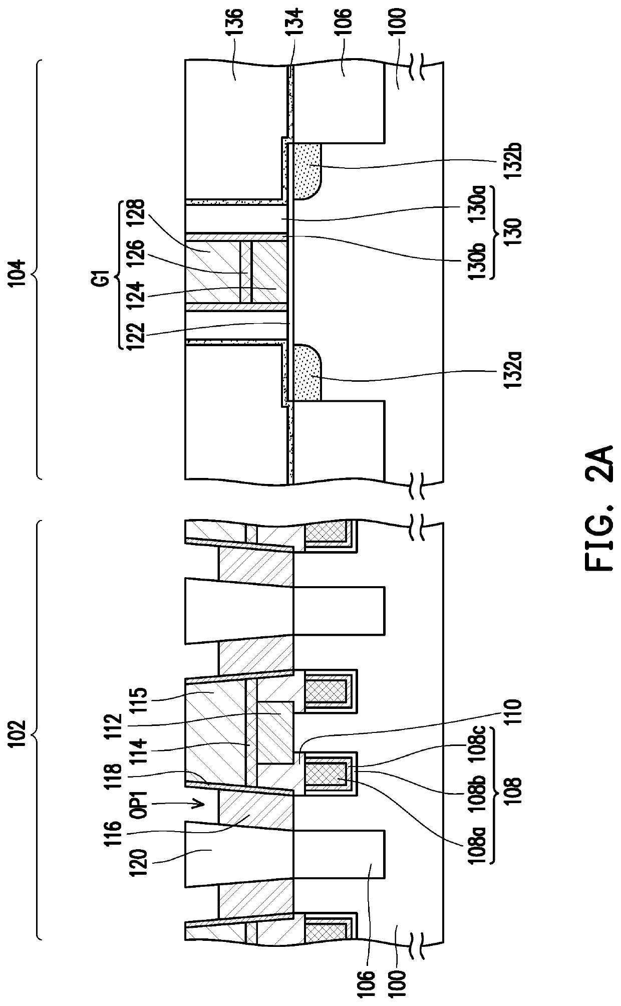
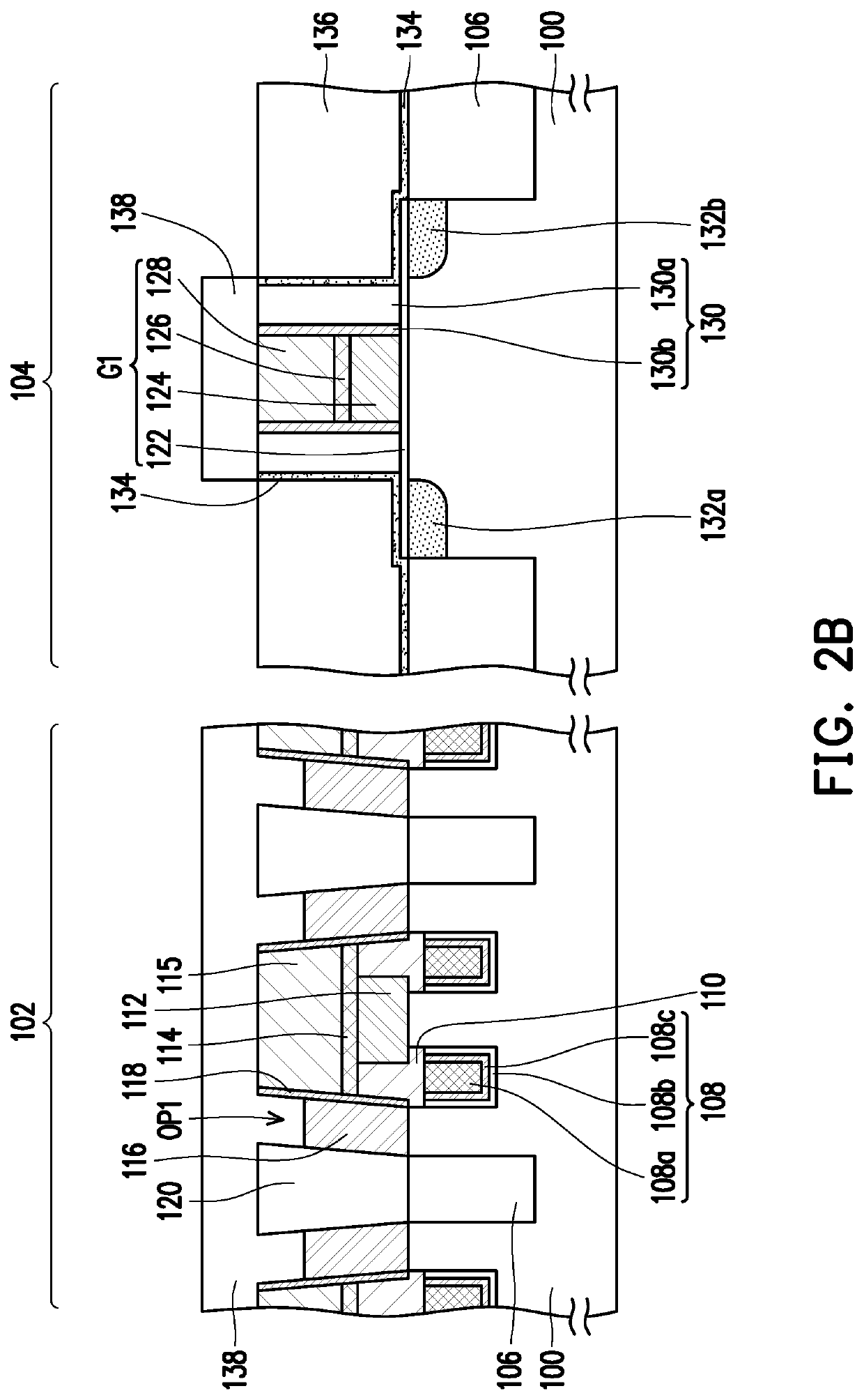
[0033]FIG. 1 is a top view illustrating some components in a memory cell region of a memory structure according to an embodiment of the invention. FIG. 2A to FIG. 2H are cross-sectional views illustrating a manufacturing process of a memory structure according to an embodiment of the invention. The memory cell region in FIG. 2A to FIG. 2H is depicted along the section line I-I′ in FIG. 1. Some components in FIG. 2A to FIG. 2H are omitted in FIG. 1 to clearly illustrate the positional relationship between the components in FIG. 1.

[0034]Referring to FIG. 1 and FIG. 2A, a substrate 100 is provided. The substrate 100 includes a memory cell region 102 and a peripheral circuit region 104. The memory cell region 102 can be used to form a memory cell (e.g., a dynamic random access memory cell (DRAM cell)), and the peripheral circuit region 104 can be used to form a transistor. The substrate 100 is, for example, a semiconductor substrate such as a silicon substrate. An isolation structure 10...


PUM

PropertyMeasurementUnit
conductiveaaaaaaaaaa
semiconductor structureaaaaaaaaaa
energyaaaaaaaaaa

Abstract

A memory structure including a substrate, a memory cell, and a transistor is provided. The substrate includes a memory cell region and a peripheral circuit region. The memory cell is located in the memory cell region. The transistor is located in the peripheral circuit region. The transistor includes a gate, a first doped region, a second doped region, a first nickel silicide layer, and a second nickel silicide layer. The gate is located on the substrate and is insulated from the substrate. The first doped region and the second doped region are located in the substrate on two sides of the gate. The first nickel silicide layer is located on an entire top surface of the first doped region, and the second nickel silicide layer is located on an entire top surface of the second doped region.

Description

CROSS-REFERENCE TO RELATED APPLICATION[0001]This application claims the priority benefit of Taiwan application serial no. 108112991, filed on Apr. 15, 2019. The entirety of the above-mentioned patent application is hereby incorporated by reference herein and made a part of this specification.BACKGROUND OF THE INVENTIONField of the Invention[0002]The invention relates to a semiconductor structure and a manufacturing method thereof, and particularly relates to a memory structure and a manufacturing method thereof.Description of Related Art[0003]Currently, the common data processing method is to perform data processing by using the memory and the processor located on different chips. However, when performing a large amount of data processing, it requires a lot of energy and time to move data back and forth between various memories and processors.[0004]Therefore, a memory structure in which the memory and the processor are integrated on the same chip has been gradually developed. Howeve...

Claims


Application Information

Patent Timeline
Patent Type & Authority Patents(United States)
IPC IPC(8): H01L27/108H01L21/223H01L29/49H01L29/66H01L21/285H01L21/28H01L29/45
CPCH01L27/10894H01L21/2236H01L21/28052H01L21/28518H01L27/10823H01L27/10876H01L27/10897H01L29/45H01L29/4933H01L29/665H10B12/315H10B12/09H10B12/50H01L29/66575H01L29/6656H01L29/7843H01L21/76889H01L21/76897H10B12/34H10B12/0335H10B12/053
Inventor CHU, YING-TSUNGCHIU, CHING-KANGHO, CHING-SUNG
Owner POWERCHIP SEMICON MFG CORP
Why Eureka
Try Eureka