

Anode and battery
a technology applied in the field of anode and battery, can solve the problem of easy decline of cycle characteristics, and achieve the effect of increasing performance, small size and more functions
- Summary
- Abstract
- Description
- Claims
- Application Information
AI Technical Summary
Benefits of technology
Problems solved by technology
Method used
Image

Examples
example 1-1
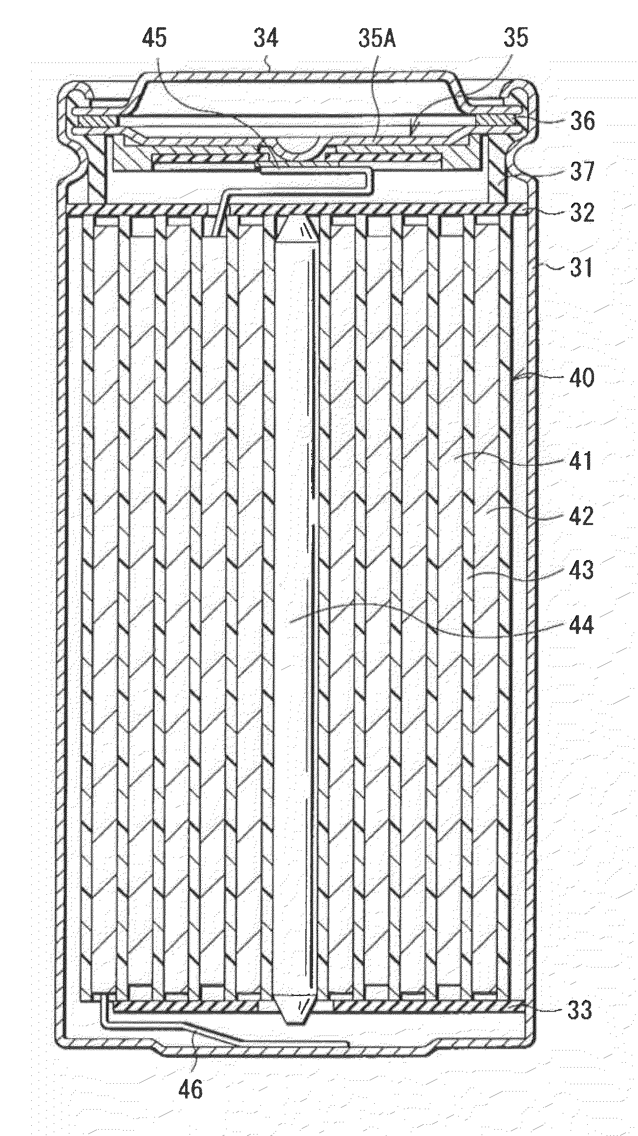
[0174]A laminate film type secondary battery shown in FIGS. 12 and 13 was manufactured by the following steps. At that time, the laminate film type secondary battery was a lithium-ion secondary battery in which the capacity of the anode 54 is represented based on insertion and extraction of lithium.
[0175]At first, the cathode 53 was formed. After lithium carbonate (Li2CO3) and cobalt carbonate (CoCO3) were mixed at a molar ratio of 0.5:1, the mixture was fired in air at 900° C. for 5 hours to obtain a lithium-cobalt complex oxide (LiCoO2). Next, after 91 parts by weight of the lithium-cobalt complex oxide as a cathode active material, 6 parts by weight of graphite as an electrical conductor and 3 parts by weight of polyvinylidene fluoride as a binder were mixed to form a cathode mixture, the cathode mixture was dispersed in N-methyl-2-pyrrolidone to form paste-form cathode mixture slurry. Finally, after the cathode mixture slurry was uniformly applied to both sides of the cathode cu...
examples 1-2 to 1-13
[0181]Secondary batteries were formed by the same steps as those in Example 1-1, except that the peak diameter was 400 nm (Example 1-2), 700 nm (Example 1-3), 800 nm (Example 1-4), 1000 nm (Example 1-5), 3000 nm (Example 1-6), 5000 nm (Example 1-7), 7000 nm (Example 1-8), 8000 nm (Example 1-9), 9000 nm (Example 1-10), 10000 nm (Example 1-11), 12000 nm (Example 1-12) or 15000 nm (Example 1-13).
examples 2-1 to 2-13
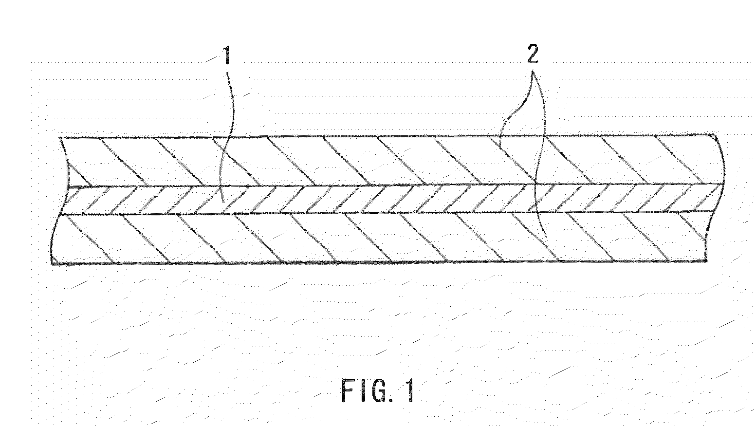
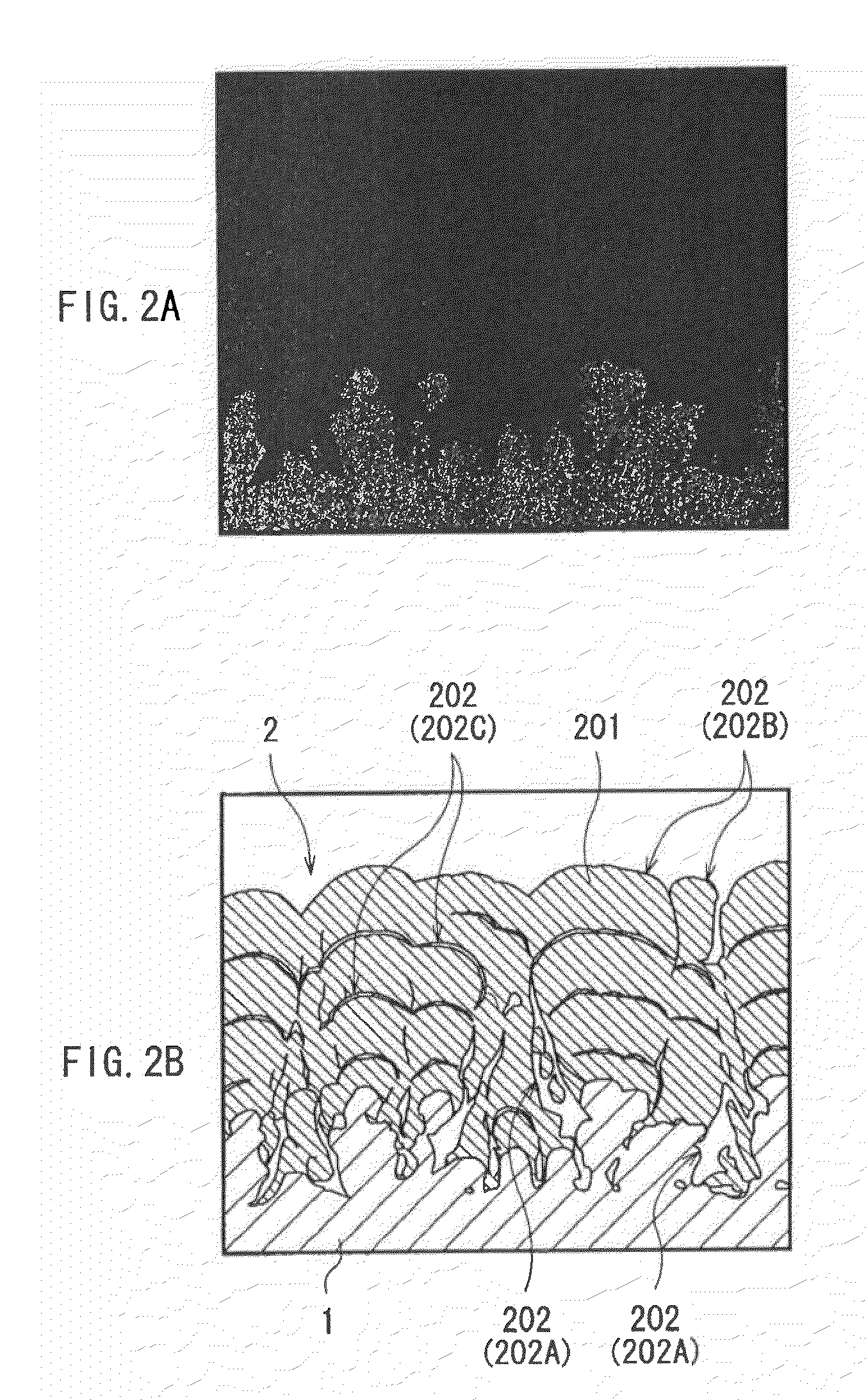
[0188]Secondary batteries were formed by the same steps as those in Examples 1-1 to 1-13, except that the anode active material had a six-layer configuration. In the case where the anode active material was formed, while the anode current collector 54A was moved back and forth relatively to an evaporation source, silicon was deposited successively, and the silicon deposition rate was 10 nm / s.
PUM
| Property | Measurement | Unit |
|---|---|---|
| diameter | aaaaa | aaaaa |
| diameter | aaaaa | aaaaa |
| diameter | aaaaa | aaaaa |
Abstract
Description
Claims
Application Information