Method for producing single crystal silicon carbide

a single crystal silicon carbide and silicon carbide technology, applied in the direction of single crystal growth, polycrystalline material growth, liquid-phase epitaxial-layer growth, etc., can solve the problem of easy generation of crystal defects, micropipe defects, crystal defects, etc., and difficult stoichiometrically accurate control of partial pressure, etc., to suppress the entry of impurities upon heat treatment

Inactive Publication Date: 2009-02-12
KWANSEI GAKUIN EDUCATIONAL FOUND
View PDF7 Cites 15 Cited by
  • Summary
  • Abstract
  • Description
  • Claims
  • Application Information

AI Technical Summary

Benefits of technology

[0031]By this method, because there is no need of treatment by dipping in melted Si, there is no permeation of excessive Si between the single crystal SiC substrate and the polycrystal SiC substrate.
[0032]In addition, by this method, entrance of impurities upon heat treatment ca...

Problems solved by technology

It is technically very difficult to stoichiometrically accurately control the partial pressures of them.
In addition, impurities are easy to mix in, and crystal defects, micropipe defects, etc., are apt to be generated under the influence of distortion caused by the mixed impurities or heat.
Thus, there is a problem that single crystal SiC stable in performance and quality can not be obtained.
Therefore, the productivity of single crystal SiC is low and the temperature of the liquid phase in the production ...

Method used


Image

  • Method for producing single crystal silicon carbide
  • Method for producing single crystal silicon carbide
  • Method for producing single crystal silicon carbide

Examples


Embodiment Construction

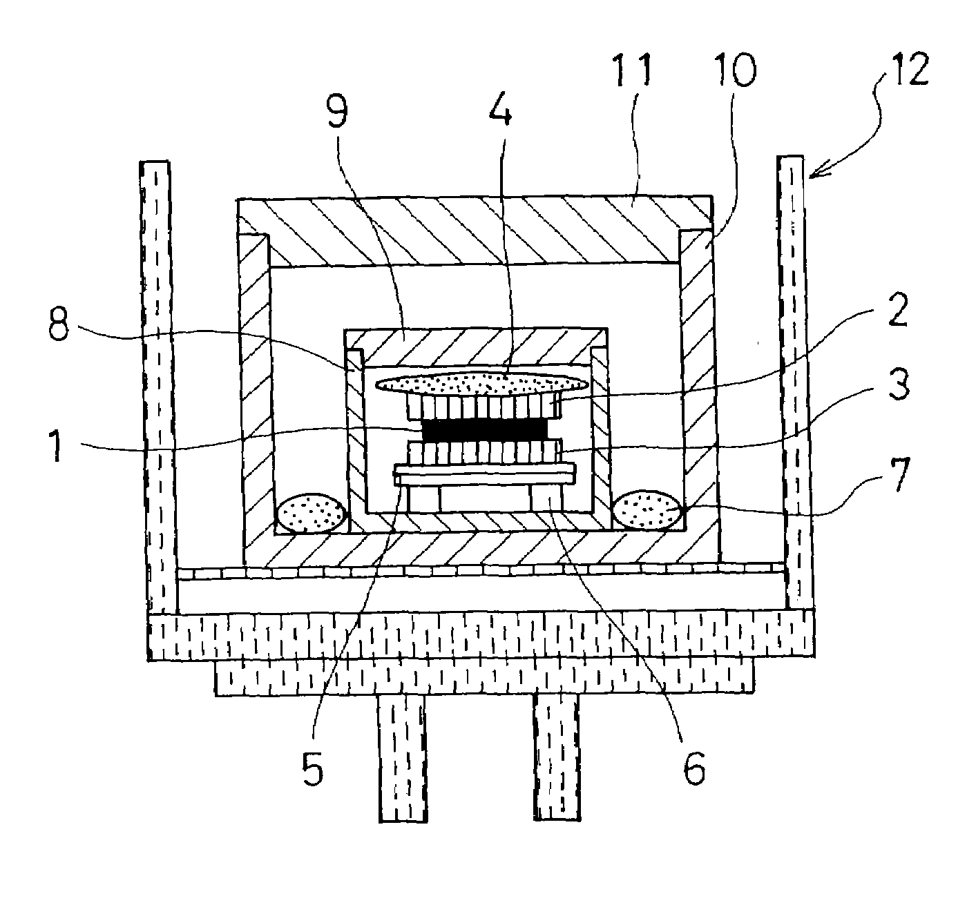
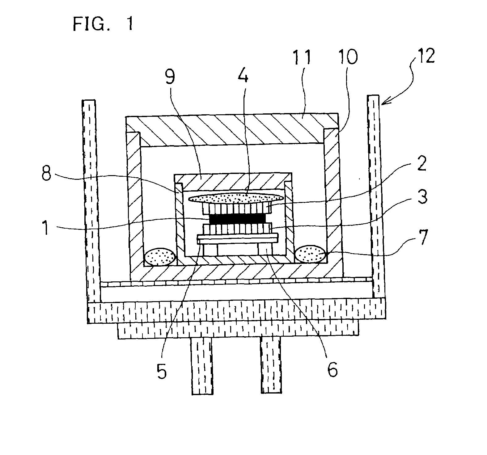
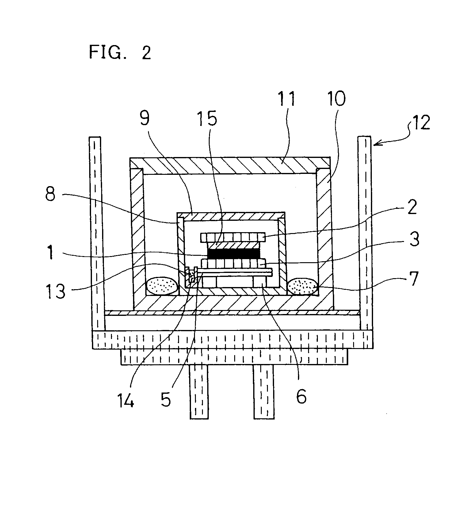
[0046]Hereinafter, single crystal SiC according to the present invention will be described with reference to FIGS. 1 and 2 using examples different in manner of interposing very thin metallic Si melt layer between single crystal and polycrystal SiC substrates.

[0047]FIG. 1 is a schematic sectional view of a heat treat furnace used for growing single crystal SiC according to the present invention. In FIG. 1, reference numeral 1 denotes a single crystal 6H-SiC substrate as a seed crystal. Reference numerals 2 and 3 denote polycrystal SiC substrates sandwiching the single crystal SiC substrate 1. Reference numeral 4 denotes metallic Si. Reference numeral 7 denotes a Si piece for controlling sublimation of SiC upon heat treatment. Reference numeral 10 denotes a crucible made of graphite. Reference numeral 11 denotes an upper cover. Reference numeral 12 denotes a soaking case.

[0048]As illustrated in FIG. 1, the single crystal SiC substrate 1, polycrystal SiC substrates 2 and 3, and metall...


PUM


Abstract

Single crystal SiC, having no fine grain boundaries, a micropipe defect density of 1/cm2 or less and a crystal terrace of 10 micrometer or more is obtained by a high-temperature liquid phase growth method using a very thin Si melt layer. The method does not require temperature difference control between the growing crystal surface and a raw material supply polycrystal and preparation of a doped single crystal SiC is possible.

Description

CROSS REFERENCE TO RELATED APPLICATIONS[0001]This application is a divisional application of prior U.S. patent application Ser. No. 10 / 479,614, filed Jun. 30, 2004, the disclosure of which is incorporated herein by reference in its entirety. The parent application is a national stage of PCT / JP01 / 04708, filed Jun. 4, 2001, the disclosure of which is incorporated herein by reference in its entirety.BACKGROUND OF THE INVENTION[0002]1. Field of the Invention[0003]The present invention relates to single crystal silicon carbide, more specifically, to single crystal silicon carbide used in broad fields as semiconductor devices such as light-emitting diodes, power devices, high-frequency devices, and environment-resistant devices.[0004]2. Description of the Related Art[0005]Silicon carbide (hereinafter referred to as SiC) is superior in heat resistance and mechanical strength, besides it has good resistance to radiation. Further, it is easy to perform valence control of electrons and holes ...

Claims


Application Information

Patent Timeline
IPC IPC(8): C30B19/00C30B19/04C30B29/36
CPCC30B29/36C30B19/04
Inventor KANEKO, TADAAKIASAOKA, YASUSHISANO, NAOKATSU
Owner KWANSEI GAKUIN EDUCATIONAL FOUND
Why Eureka
Try Eureka