Electron microscope

a technology of electron beam and charge particle, which is applied in the direction of material analysis using wave/particle radiation, instruments, photomechanical devices, etc., can solve the problem of difficult measurement of charge amount prior to irradiation of electron beam, and achieve the effect of eliminating the potential gradient of the observation region and high spatial resolution

Inactive Publication Date: 2009-02-12
HITACHI HIGH-TECH CORP
View PDF6 Cites 17 Cited by
  • Summary
  • Abstract
  • Description
  • Claims
  • Application Information

AI Technical Summary

Benefits of technology

[0031]If the technique in accordance with the present invention is used, the distribution of the charging potential can be measured with high spatial resolution without irradiation of the primary electron beam onto the sample. Consequently, the present invention can be applied to measuring the potential gradient of the observation region prior to observation. If observation coordinates is compensated based on the result of measurement of the potential gradient, the desired observation region can be observed. Further, as is exhibited in FIG. 10, the influence of drift of an image by charging is inhibited and the bottom of the contact hole with a high aspect ratio becomes possible to be observed by performing the preliminary irradiation again to eliminate the potential gradient of the observation region. This method is effective not only for observation of the bottom of the contact hole but also for general technique wherein observation is performed after preliminary charging.
[0032]According to the constitution described above, observation of the sample inhibiting the influence of charging by irradiation of an electron beam is possible, because the potential of the sample is detected from the information obtained under the state the charged particle beam is not incident on the sample and optical conditions are controlled.

Problems solved by technology

Although both of the techniques described in the patent documents 1 and 2 relate to the technique wherein a charged amount on a sample is measured and conditions of a device are adjusted based on the measurement, because the charged amount is measured by detecting a signal obtained according to irradiation of an electron beam to the sample, charging is forcibly induced by irradiation of the electron beam, and a problem that measurement of the charged amount prior to irradiation of the electron beam is difficult is involved.
On the other hand, according to the technique described in the patent document 3, although measurement of a potential of the sample surface is possible without inducing charging by an electron beam, there are problem that it takes time to make the metal needle get close to a sample, and problems of change of a potential of the sample by making the metal needle get close to the sample and discharging in the case charge amount is large.

Method used


Image

  • Electron microscope
  • Electron microscope
  • Electron microscope

Examples


first embodiment

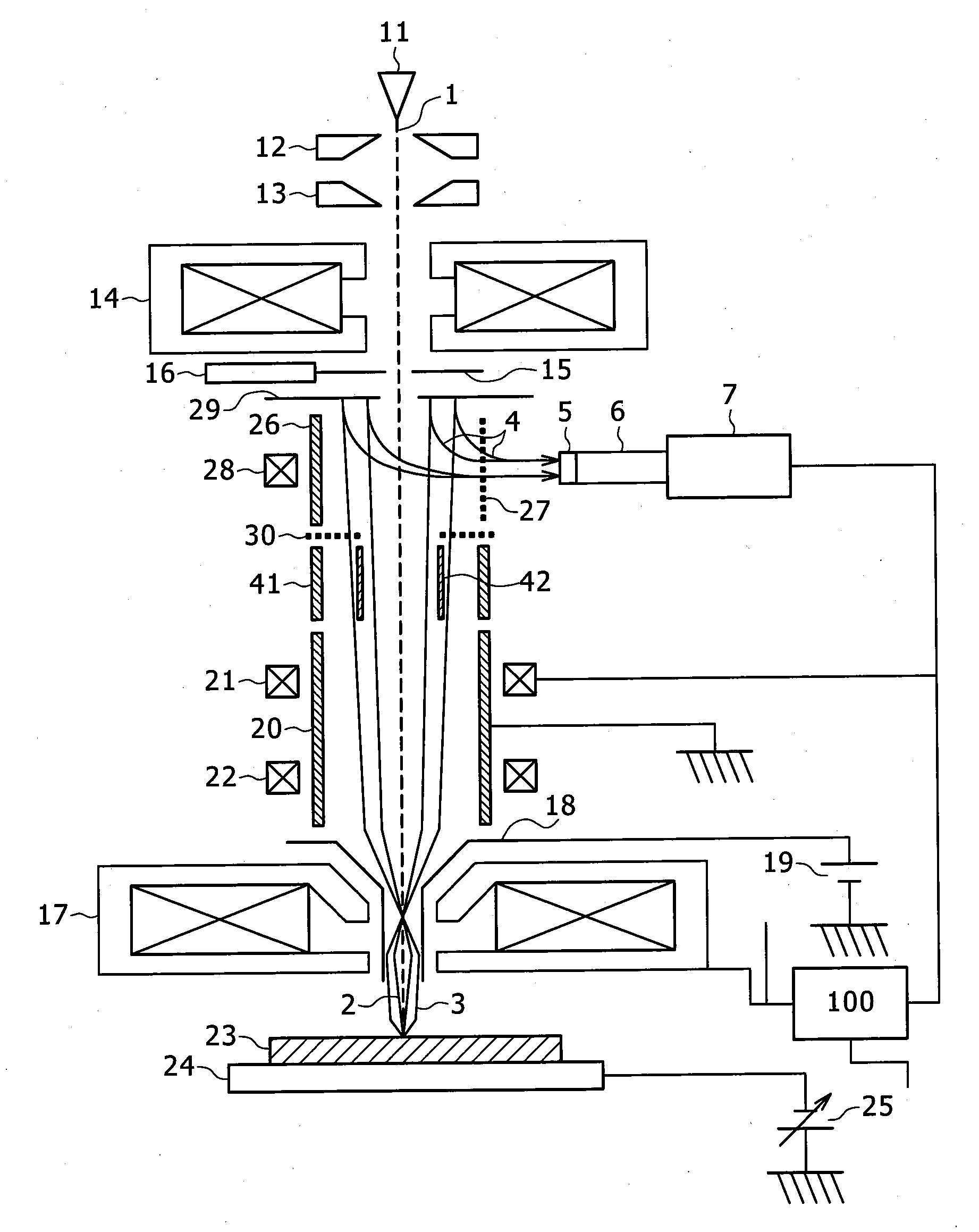
[0059]A method for measuring a potential of a sample using an electron beam will be described below.

[0060]A flowchart of the present embodiment is shown in FIG. 6. Also, an outline of a charging control device is shown in FIG. 8.

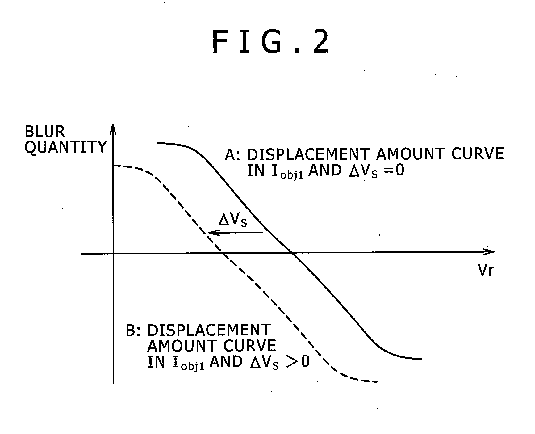
[0061]In the step S1, judgment is made whether the reference function FR of the acquisition condition to be compensated this time has been stored or not in the reference function record part 102. If there is no reference data required for the compensation this time in the record part 102, the reference sample or the uncharged sample is made a mirror state in the step S100 in the loop 1 with the condition stored in the acquisition condition record part 103 being set, and the displacement amount or the magnification against Vr is detected by a feature amount arithmetic unit 101 in the step S120. The reference function FR obtainable by function fitting using the obtained displacement amount or the magnification is obtained in the step S130, and is stored in the...

second embodiment

[0063]A flowchart of the second embodiment is shown in FIG. 7. Also, an outline of a charging control device is shown in FIG. 8.

[0064]In the step S1, judgment is made whether the reference function FR of the acquisition condition to be compensated this time has been stored or not in the reference function record part 102. If there is no reference data required for the compensation this time in the record part 102, the reference sample or the uncharged sample is made a mirror state in the step S100 in the loop 1 with the condition stored in the acquisition condition record part 103 being set, and the displacement amount or the magnification against Vr is detected by a feature amount arithmetic unit 101 in the step S120. The reference function FR obtainable by function fitting using the obtained displacement amount or the magnification is obtained in the step S130, and is stored in the reference function record part 102 in the step S140. When the reference function FR has been obtaine...


PUM

PropertyMeasurementUnit
scanning electron microscopeaaaaaaaaaa
energyaaaaaaaaaa
reflection electronaaaaaaaaaa

Abstract

Disclosed herein are a method for applying, while a charged particle beam is in a state being irradiated toward the sample, a voltage to the sample so that the charged particle beam does not reach the sample (hereafter such state may be referred to as a mirror state) and detecting information on a potential of a sample using a signal obtained then, and a device for automatically adjusting conditions of the device based on the result of measuring.

Description

BACKGROUND OF THE INVENTION[0001]1. Field of the Invention[0002]The purpose of the present invention is to provide a charged particle beam device suitable for reducing focus offset, magnification fluctuation and measurement length error in the charged particle beam device caused by charging on a sample.[0003]2. Description of the Related Art[0004]Recently, as semi-conductor devices, particularly, progress, measuring and inspecting technique of a semi-conductor is more and more increasing its importance. A scanning electron microscope represented by a CD-SEM (Critical Dimension-Scanning Electron Microscope) is a device for measuring the pattern formed on a semi-conductor device by scanning an electron beam on a sample and detecting electrons such as secondary electrons or the like emitted from the sample. In such a device, although the condition of the device is required to be appropriately set to carry out highly accurate measurement and inspection, among recent devices, there are s...

Claims


Application Information

Patent Timeline
Patent Type & Authority Applications(United States)
IPC IPC(8): G01N23/00
CPCH01J37/21H01J37/244H01J37/28H01J37/3045H01J2237/30461H01J2237/2594H01J2237/28H01J2237/2816H01J2237/24564
Inventor IKEGAMI, AKIRAYAMAZAKI, MINORUKAZUMI, HIDEYUKITAKEUCHI, KOICHIROMURAKOSHI, HISAYA
Owner HITACHI HIGH-TECH CORP
Why Eureka
Try Eureka