Display device and electronic device having the display device, and method for manufacturing thereof

a display device and electronic device technology, applied in the direction of semiconductor devices, electrical devices, transistors, etc., can solve the problems of increased cost, reduced yield, and complex crystallization process of semiconductor films, so as to suppress the increase of parasitic capacitance, suppress the reduction of yield, and suppress the effect of production cos

Inactive Publication Date: 2009-02-12
SEMICON ENERGY LAB CO LTD
View PDF4 Cites 28 Cited by
  • Summary
  • Abstract
  • Description
  • Claims
  • Application Information

AI Technical Summary

Benefits of technology

[0007]A thin film transistor using a polycrystalline semiconductor film has advantages in that mobility is two or more orders of magnitude greater than that of a thin film transistor using an amorphous semiconductor film, and a pixel portion of a display device and peripheral driver circuits thereof can be formed over the same substrate. However, the process for crystallization of a semiconductor film is more complex than that in the case of using an amorphous semiconductor film. Accordingly, there are problems in that yield is decreased and cost is increased.

Problems solved by technology

However, the process for crystallization of a semiconductor film is more complex than that in the case of using an amorphous semiconductor film.
Accordingly, there are problems in that yield is decreased and cost is increased.
There is also a problem in that the surface of a microcrystalline semiconductor film is likely to be oxidized.
Therefore, when crystal grains in a channel formation region are oxidized, oxide films are formed on the surfaces of the crystal grains and the oxide films become obstacles to carrier transfer, which causes a problem in that electric characteristics of a thin film transistor are impaired.
In addition, there is a problem in that it is difficult to increase the thickness of the microcrystalline semiconductor film as compared to that of an amorphous semiconductor film or of a polycrystalline semiconductor film and parasitic capacitance between a gate electrode and a source electrode and / or a drain electrode is caused to be increased.
From the viewpoint of improvement in aperture ratio of a pixel, while a thin film transistor having an inverted staggered structure is expected to have high performance and to be downsized, there is a problem in that leakage current (also referred to as off-current) flowing between a source region and a drain region is increased when the thin film transistor is in an off state.
Therefore, there is a problem in that it is difficult to downsize the size of the thin film transistor, to reduce a storage capacitor, and to decrease power consumption.

Method used


Image

  • Display device and electronic device having the display device, and method for manufacturing thereof
  • Display device and electronic device having the display device, and method for manufacturing thereof
  • Display device and electronic device having the display device, and method for manufacturing thereof

Examples


embodiment mode 1

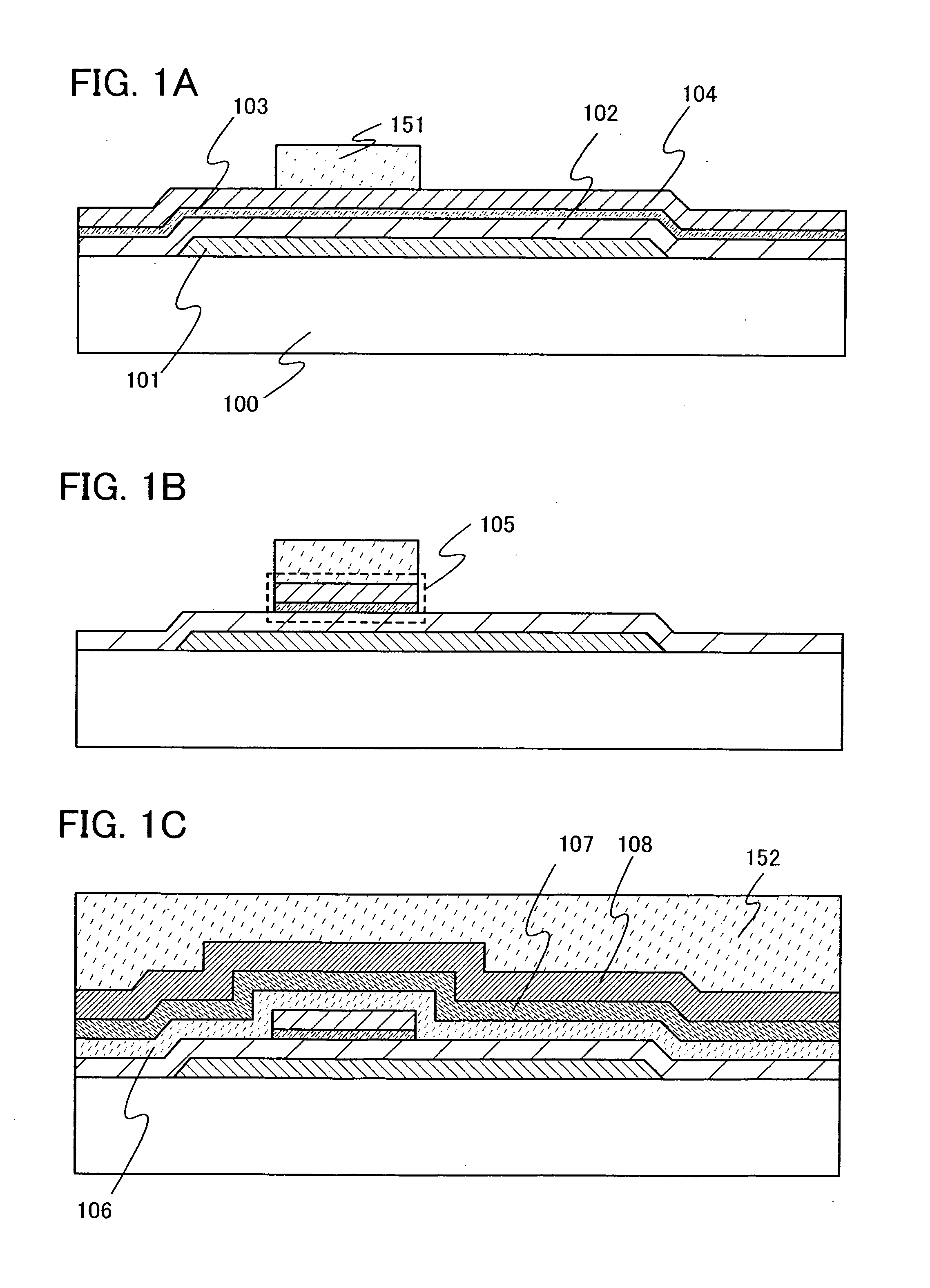
[0041]In this embodiment mode, manufacturing processes of thin film transistors used for a display device will be described with reference to FIGS. 1A to 1C, FIGS. 2A to 2C, FIGS. 3A to 3C, FIG. 4, and FIGS. 5A to 5C. FIGS. 1A to 1C, FIGS. 2A to 2C, FIGS. 3A to 3C, and FIG. 4 are cross-sectional views illustrating manufacturing processes of thin film transistors, and FIGS. 5A to 5C are top views each illustrating a connection region of a thin film transistor in one pixel of a display device and a pixel electrode.

[0042]A thin film transistor having a microcrystalline semiconductor film, which is of an n type, is more suitable for use in a driver circuit than that of a p type because it has higher mobility. It is desired that all thin film transistors formed over the same substrate have the same polarity, in order to reduce the number of steps. Here, description is made using n-channel thin film transistors.

[0043]As shown in FIG. 1A, a gate electrode 101 is formed over a substrate 100...

embodiment mode 2

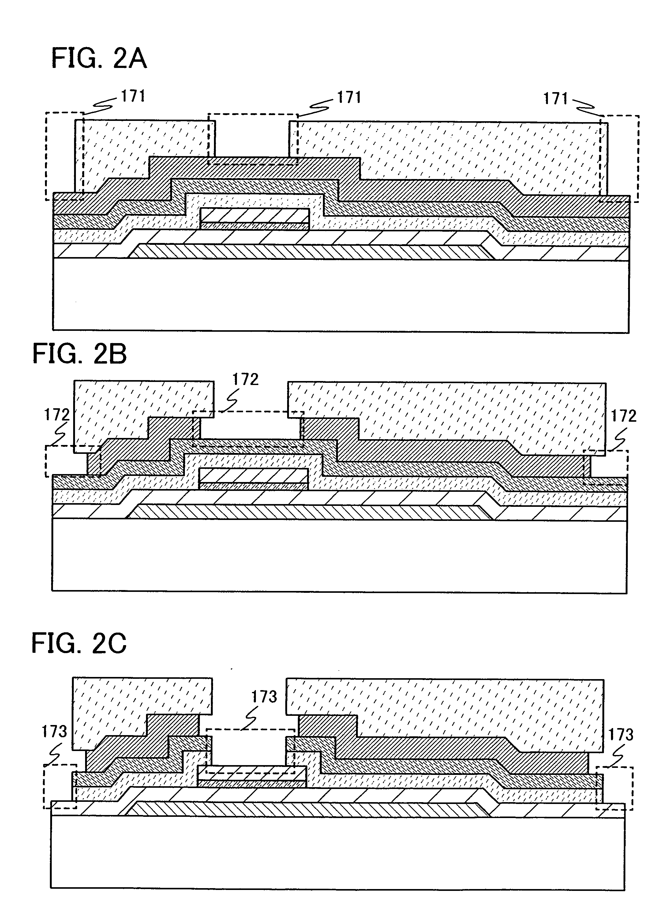
[0080]In this embodiment mode, a thin film transistor used for a display device, which is different from that described in Embodiment Mode 1, will be described with reference to FIG. 13. FIG. 13 is a cross-sectional view of a thin film transistor. Note that, in this embodiment mode, portions that are similar to the portions in Embodiment Mode 1 are denoted by the same reference numerals and description is made below with reference to the description of Embodiment Mode 1.

[0081]Note that the thin film transistor described in this embodiment mode is an n-channel thin film transistor similarly to the case of Embodiment Mode 1.

[0082]First, the gate electrode 101, the gate insulating film 102, the microcrystalline semiconductor film 103, the channel protection layer 104 are formed over the substrate 100, and a state shown in FIG. 1B of Embodiment Mode 1 is obtained by a resist mask and an etching process. The substrate 100, the gate electrode 101, the gate insulating film 102, the microcr...

embodiment mode 3

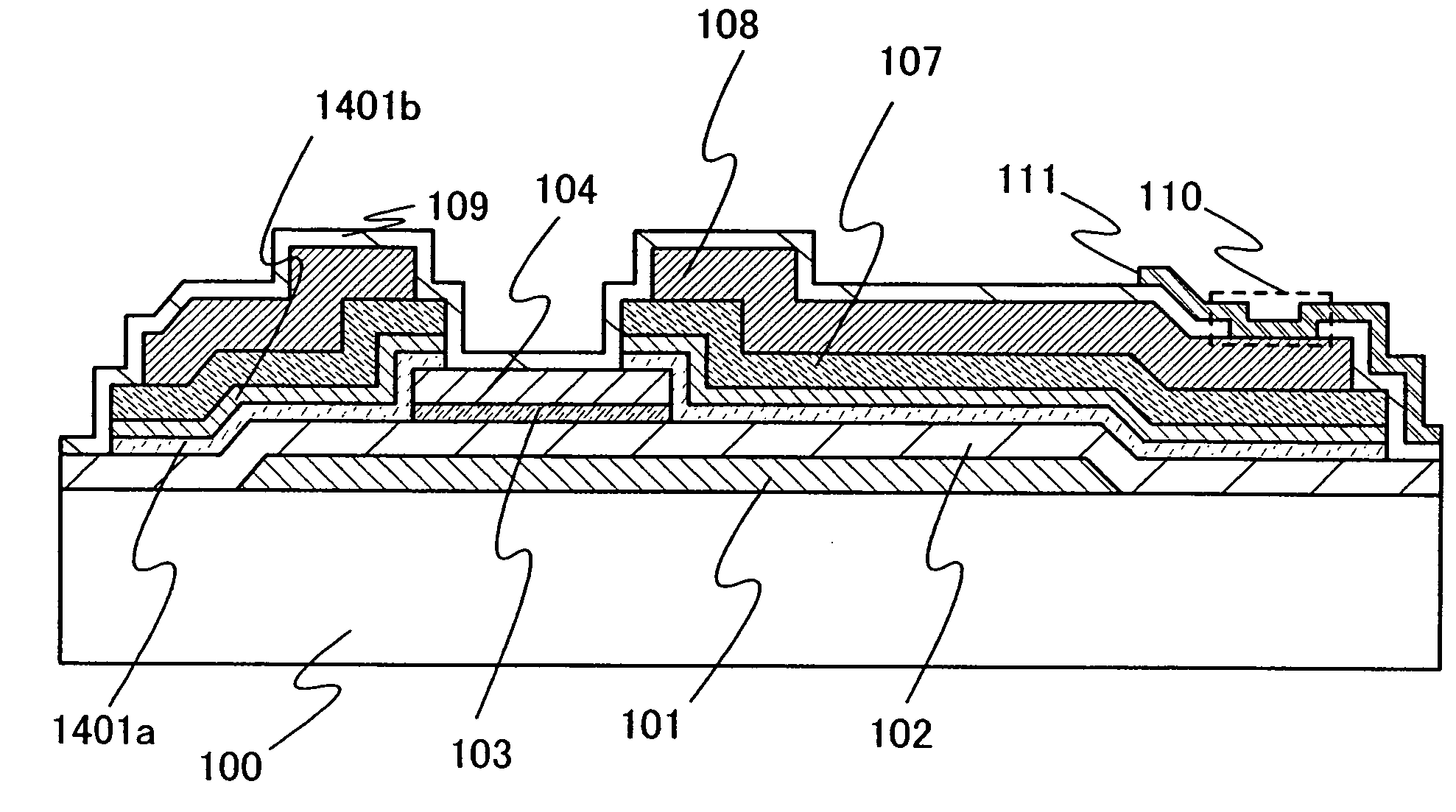
[0086]In this embodiment mode, a thin film transistor used for a display device, which is different from those described in Embodiment Mode 1 and Embodiment Mode 2, will be described with reference to FIG. 14. FIG. 14 is a cross-sectional view of a thin film transistor. Note that, in this embodiment mode, portions that are similar to the portions in Embodiment Mode 1 are denoted by the same reference numerals and description is made below with reference to the description of Embodiment Mode 1.

[0087]Note that the thin film transistor described in this embodiment mode is an n-channel thin film transistor, similarly to the case of Embodiment Mode 1.

[0088]First, the gate electrode 101, the gate insulating film 102, the microcrystalline semiconductor film 103, the channel protection layer 104 are formed over the substrate 100, and a state shown in FIG. 1B of Embodiment Mode 1 is obtained by a resist mask and an etching process. The substrate 100, the gate electrode 101, the gate insulati...


PUM


Abstract

To provide a display device including a thin film transistor in which high electric characteristics and reduction in off-current can be achieved. The display device having a thin film transistor includes a substrate, a gate electrode provided over the substrate, a gate insulating film provided over the gate electrode, a microcrystalline semiconductor film provided over the gate electrode with the gate insulating film interposed therebetween, a channel protection layer which is provided over and in contact with the microcrystalline semiconductor film, an amorphous semiconductor film provided over the gate insulating film and on a side surface of the microcrystalline semiconductor film and the channel protection layer, an impurity semiconductor layer provided over the amorphous semiconductor film, and a source electrode and a drain electrode provided over and in contact with the impurity semiconductor layer. The thickness of the amorphous semiconductor film is larger than that of the microcrystalline semiconductor film.

Description

BACKGROUND OF THE INVENTION[0001]1. Field of the Invention[0002]The present invention relates to a display device and an electronic device using the display device. In particular, the present invention relates to a display device using a thin film transistor in a pixel portion and an electronic device using the display device.[0003]2. Description of the Related Art[0004]In recent years, techniques that are used to form thin film transistors using a semiconductor thin film (with a thickness of approximately several nanometers to several hundreds of nanometers) which is formed over a substrate with an insulating surface have been put into practice in many electronic devices. In particular, thin film transistors have been put into practical use as switching elements in a pixel portion of a display device, and research and development has been actively conducted.[0005]As a switching element of a liquid crystal display device, a thin film transistor using an amorphous semiconductor film ...

Claims


Application Information

Patent Timeline
Patent Type & Authority Applications(United States)
IPC IPC(8): H01L33/00H01L21/00H01L21/336H01L29/786
CPCH01L29/04H01L29/78696H01L29/66765H01L29/41733H01L29/458H01L29/78606
Inventor KOBAYASHI, SATOSHIMIYAGUCHI, ATSUSHIMORIYA, YOSHITAKAKUROKAWA, YOSHIYUKIKAWAE, DAISUKE
Owner SEMICON ENERGY LAB CO LTD
Why Eureka
Try Eureka