
Double exposure semiconductor process for improved process margin

Active Publication Date: 2009-02-12
XILINX INC
View PDF11 Cites 5 Cited by
  • Summary
  • Abstract
  • Description
  • Claims
  • Application Information

AI Technical Summary

Benefits of technology

[0011]To overcome limitations in the prior art, and to overcome other limitations that will become apparent upon reading and understanding the present specification, various embodiments of the present invention disclose a double exposure semiconductor process for improved process margin.

Problems solved by technology

Obtaining 50 nm feature sizes using conventional single exposure processes, however, is challenging.
Unfortunately, the photoresist trimming process also produces an undesirable reduction in the sizes of other critical feature patterns, such as poly-to-contact enclosure patterns and field poly width, thereby increasing the poly-to-contact and field poly line resistance beyond acceptable process margins.

Method used


Image

  • Double exposure semiconductor process for improved process margin
  • Double exposure semiconductor process for improved process margin
  • Double exposure semiconductor process for improved process margin

Examples


Embodiment Construction

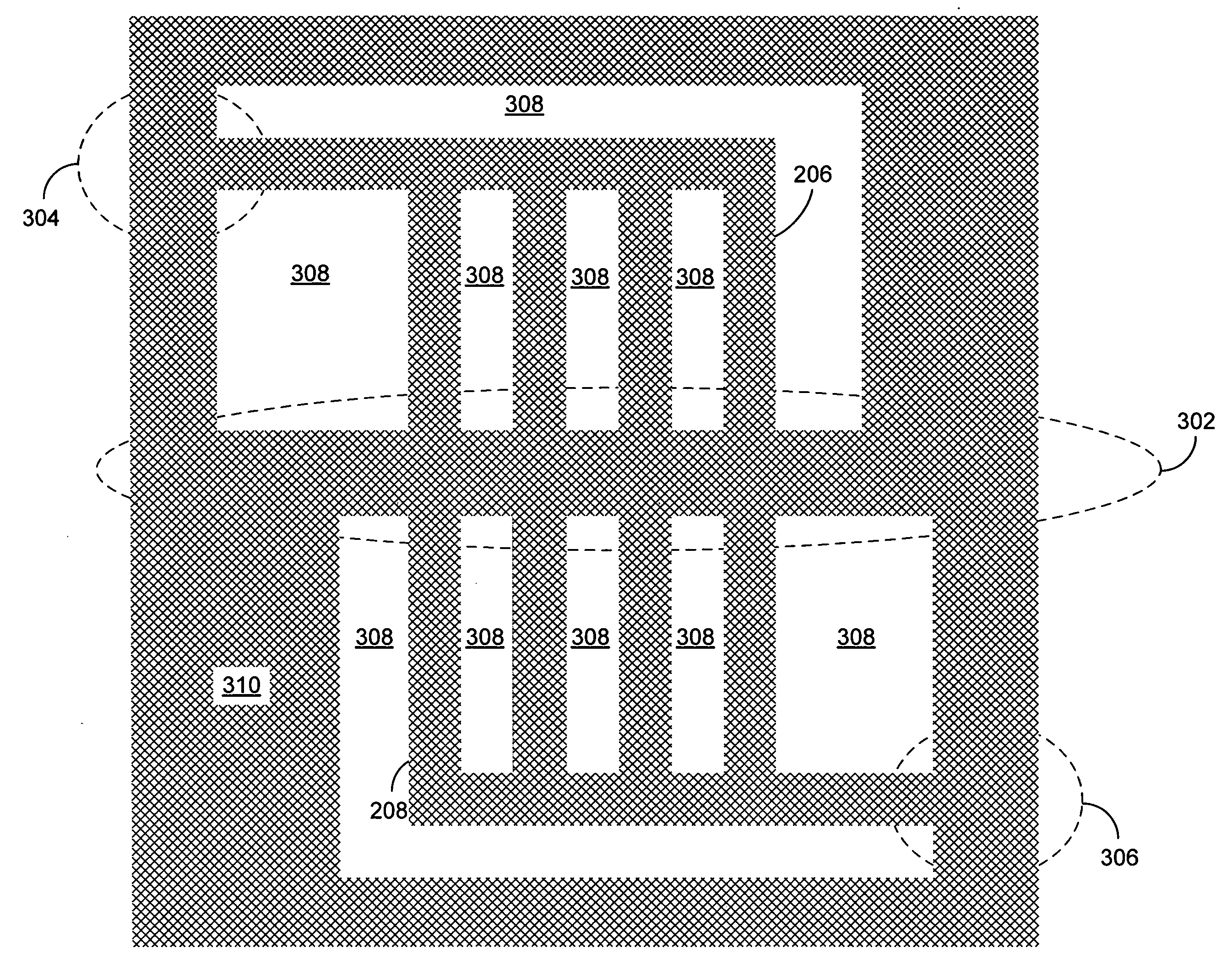
[0023]Generally, various embodiments of the present invention provide a double exposure semiconductor process for improved process margin at nanometer feature sizes. In one embodiment of the present invention, a starting material comprising various layers, such as a silicon or germanium substrate, silicon dioxide, polycrystalline silicon (polysilicon), hard mask, and bottom anti-reflective coating (BARC) is formed on a semiconductor wafer (wafer). Next, a photoresist layer is spin-coated on the wafer to produce a uniform, adherent, defect-free, polymeric film of a desired thickness over the entire wafer.

[0024]The wafer is then soft-baked, so as to drive solvent out of the spun-on photoresist and to relieve photoresist film stresses encountered by the spinning process. Next, a first exposure process is used to create an exposed image in the photoresist to define certain device features within the photoresist. A subsequent photoresist development and trimming process is then executed ...


PUM

PropertyMeasurementUnit
Transmissionaaaaaaaaaa
Widthaaaaaaaaaa
Heightaaaaaaaaaa

Abstract

A double exposure semiconductor process is provided for improved process margin at reduced feature sizes. During a first processing sequence, features defining non-critical dimensions of a polysilicon interconnect structure are formed, while other portions of the polysilicon layer are left un-processed. During a second processing sequence, features that define the critical dimensions of the polysilicon interconnect structure are formed without the need to execute a photoresist trimming procedure. Accordingly, only an etch process is executed, which provides higher resolution processing to create the critical dimensions needed during the second processing sequence.

Description

FIELD OF THE INVENTION[0001]The present invention generally relates to advanced semiconductor processing, and more particularly, to a microlithographic exposure process for improved process margin.BACKGROUND OF THE INVENTION[0002]Advances in the field of semiconductor integrated circuits have brought about higher levels of integration. Accordingly, semiconductor manufacturing process advancements are driving the corresponding geometric dimensions of semiconductor devices to decreasingly smaller values. 10 micrometer (μm) gate lengths, for example, were common in the 1970's, but continuously advancing semiconductor manufacturing processes have reduced gate lengths to well below 100 nanometer (nm).[0003]Continuing efforts to achieve higher levels of integration have also led to reductions in the separation distance between adjacent semiconductor features. For example, nanometer processes producing 65 nm and 45 nm gate lengths require a device spacing of, e.g., 120 nm to achieve reason...

Claims


Application Information

Patent Timeline
IPC IPC(8): H01L21/461G03C5/00
CPCG03F7/0035G03F7/40G03F7/2024
Inventor HO, JONATHAN JUNG-CHING
Owner XILINX INC
Features
  • Generate Ideas
  • Intellectual Property
  • Life Sciences
  • Materials
  • Tech Scout
  • Unparalleled Data Quality
  • Higher Quality Content
  • 60% Fewer Hallucinations
Learn More