Semiconductor device and manufacturing method thereof

a semiconductor film and semiconductor technology, applied in the direction of semiconductor devices, basic electric elements, electrical appliances, etc., can solve the problems of difficult to obtain a film with a uniform crystalline structure, easy oxidation of the surface of the crystal grain of the microcrystalline semiconductor film, etc., to achieve the effect of improving the electric characteristi

Inactive Publication Date: 2009-02-19
SEMICON ENERGY LAB CO LTD
View PDF40 Cites 27 Cited by
  • Summary
  • Abstract
  • Description
  • Claims
  • Application Information

AI Technical Summary

Benefits of technology

[0014]The microcrystalline semiconductor layer including the acceptor impurity element is formed, whereby the threshold voltage of the thin film transistor can be controlled. Addition of the acceptor impurity element is effective for an n-channel thin film transistor. For example, a gas selected from trimethylboron, B2H6, BF3, BCl3, and BBr3 can be used for the dop

Problems solved by technology

However, an amorphous semiconductor film is crystallized with a laser beam to form the polycrystalline semiconductor film, and thus there are problems in that it is difficult to obtain a film with a uniform crystalline s

Method used


Image

  • Semiconductor device and manufacturing method thereof
  • Semiconductor device and manufacturing method thereof
  • Semiconductor device and manufacturing method thereof

Examples


embodiment modes

[0035]Hereinafter, embodiment modes of the present invention are described. It is easily understood by those skilled in the art that the present invention can be carried out in many different modes, and the modes and details disclosed herein can be modified in various ways without departing from the spirit and scope of the present invention. Therefore, the present invention should not be interpreted as being limited to the description of the embodiment modes to be given below. Further, the same reference numeral in different drawings represents the same component, and repeated description of a material, a shape, a manufacturing method, or the like is omitted.

embodiment mode 1

[0036]This embodiment mode describes a structure of a thin film transistor used in a semiconductor device in the present invention and a manufacturing method thereof. Specifically, this embodiment mode describes a bottom gate thin film transistor (TFT) with a channel-etched structure and a manufacturing method thereof.

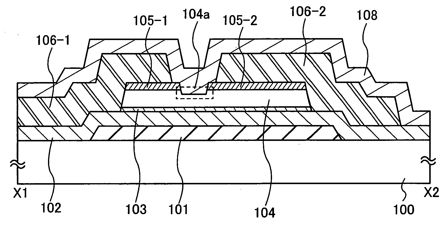
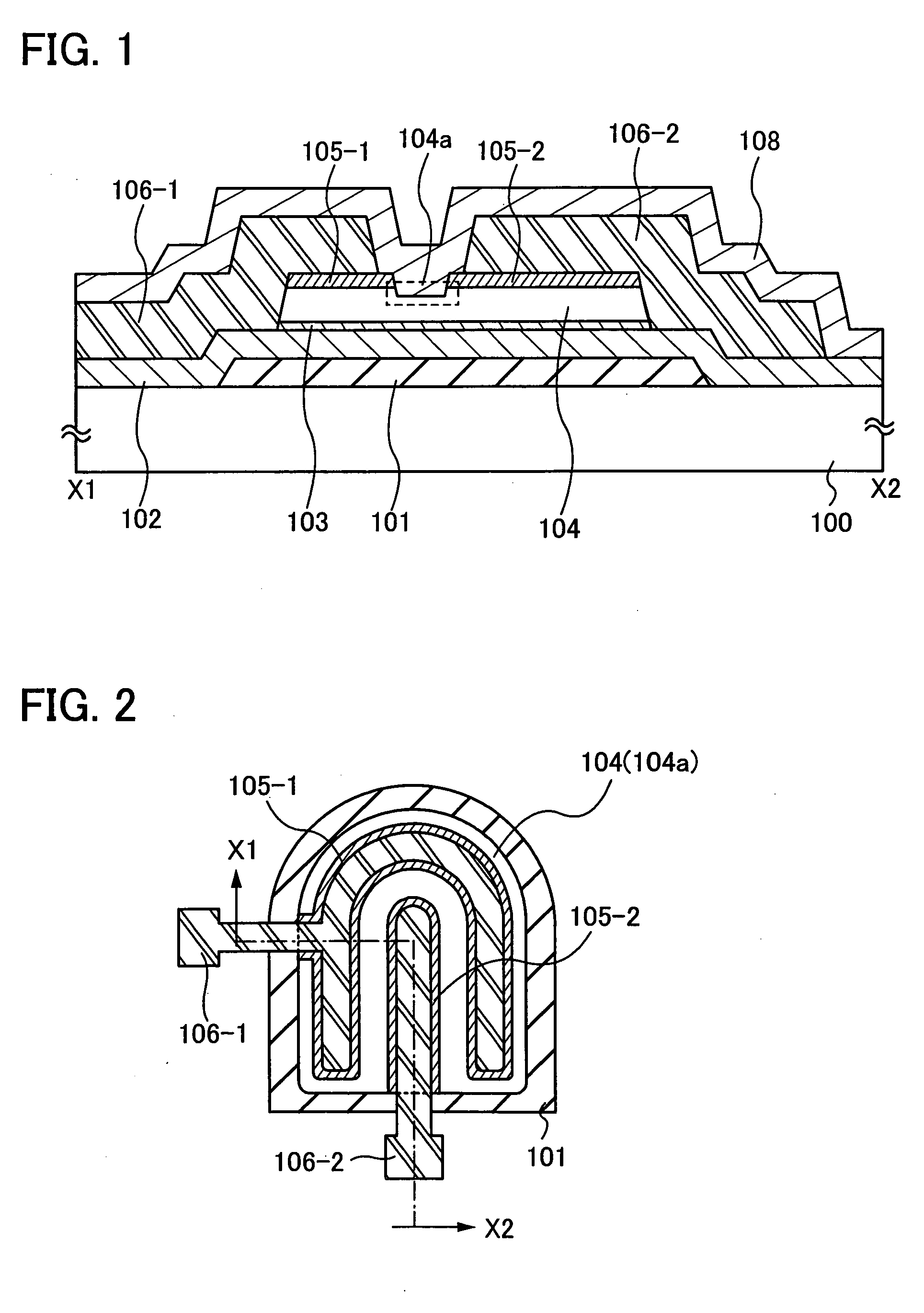
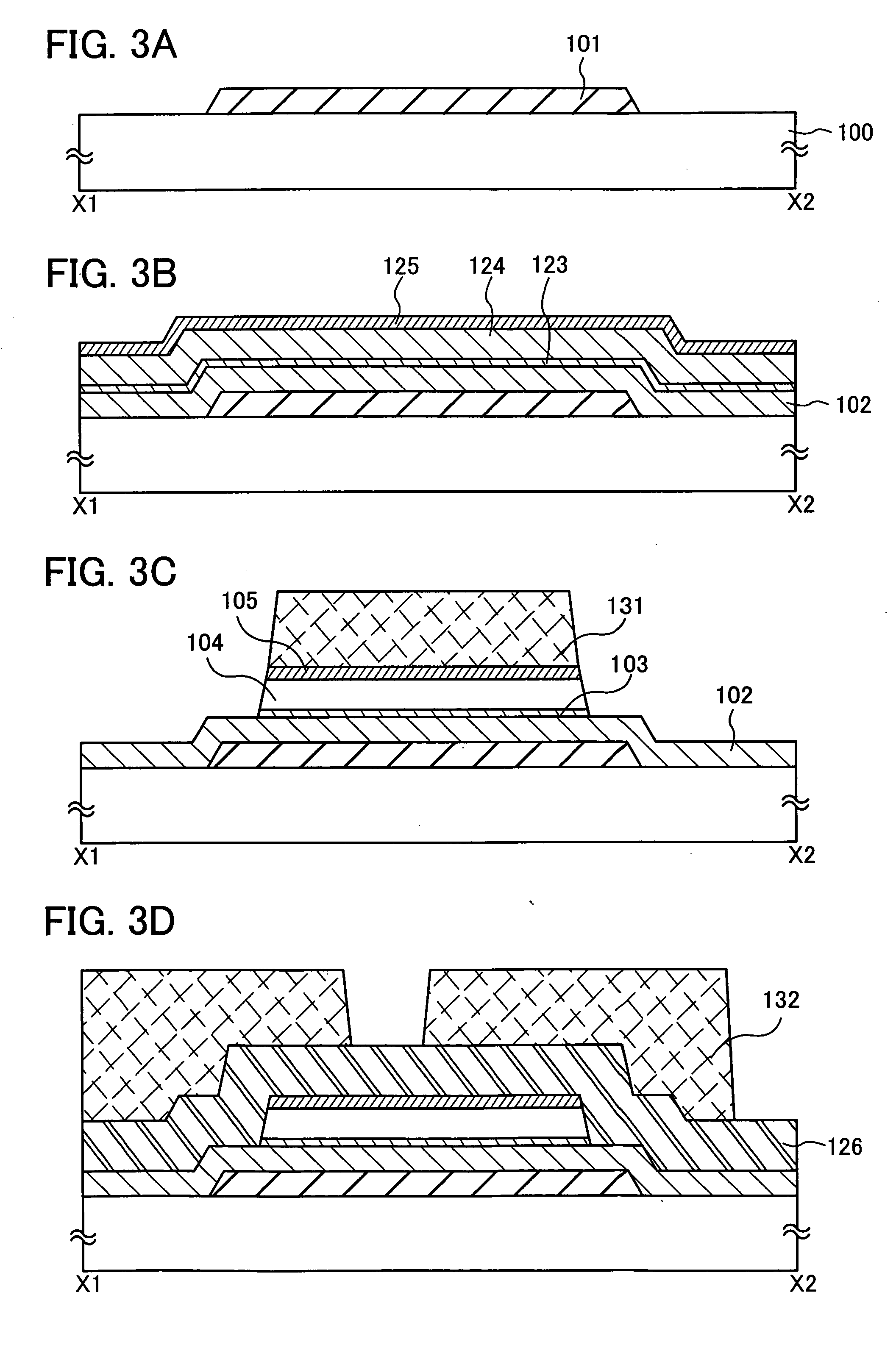
[0037]FIG. 1 is a cross-sectional view illustrating an example of a structure of the TFT, and FIG. 2 is a top view thereof. FIG. 1 is a cross-sectional view taken along a line X1-X2 in FIG. 2.

[0038]The TFT is formed over a substrate 100. In the TFT, a first conductive layer 101, an insulating layer 102, a first semiconductor layer 103, a second semiconductor layer 104, and a pair of third semiconductor layers 105-1 and 105-2 are stacked in this order over the substrate 100. The first conductive layer 101 forms a gate electrode of the TFT. The insulating layer 102 forms a gate insulating layer of the TFT. The first semiconductor layer 103 is formed of a microcrystalline...

embodiment mode 2

[0092]This embodiment mode describes a thin film transistor with a different structure from Embodiment Mode 1, and a manufacturing method thereof. This embodiment mode describes a thin film transistor having a protective layer formed of an insulating film over a channel formation region, whereas Embodiment Mode 1 shows a channel-etched thin film transistor. Such a structure of a TFT having a protective layer is called a “channel-protective type.”FIG. 5 is a cross-sectional view illustrating an example of a structure of a channel-protective TFT, and FIG. 6 is a top view thereof. FIG. 5 is a cross-sectional view taken along a line Y1-Y2 in FIG. 6.

[0093]The TFT in this embodiment mode is different from the TFT in Embodiment Mode 1 in the following point: the second semiconductor layer 104 is not provided with the recessed portion 104a but is provided with a protective layer 109 thereover; further, as shown in FIG. 6, the second semiconductor layer 104 is not exposed but is covered with...


PUM


Abstract

The present invention relates to a semiconductor device including a thin film transistor comprising a microcrystalline semiconductor which forms a channel formation region and includes an acceptor impurity element, and to a manufacturing method thereof. A gate electrode, a gate insulating film formed over the gate electrode, a first semiconductor layer which is formed over the gate insulating film and is formed of a microcrystalline semiconductor, a second semiconductor layer which is formed over the first semiconductor layer and includes an amorphous semiconductor, and a source region and a drain region which are formed over the second semiconductor layer are provided in the thin film transistor. A channel is formed in the first semiconductor layer when the thin film transistor is placed in an on state.

Description

BACKGROUND OF THE INVENTION[0001]1. Field of the Invention[0002]The present invention relates to a semiconductor device including a thin film transistor, and to a manufacturing method thereof.[0003]2. Description of the Related Art[0004]A technique in which a thin film transistor is formed using a thin semiconductor film (with a thickness of from several nm to several hundreds of nm, approximately) formed over a substrate having an insulating surface is known. Thin film transistors are widely applied to electronic devices such as integrated circuits or active matrix liquid crystal display devices. In an active matrix liquid crystal display device, thin film transistors are used as switching elements of pixels. An amorphous silicon film, a polycrystalline silicon film, a microcrystalline silicon film, or the like is used for a thin semiconductor film of this thin film transistor.[0005]An amorphous silicon film used in a thin film transistor is generally formed by a plasma-enhanced ch...

Claims


Application Information

Patent Timeline
IPC IPC(8): H01L21/20H01L29/04
CPCH01L29/04H01L29/78696H01L29/66765H01L29/41733
Inventor YAMAZAKI, SHUNPEIFURUNO, MAKOTO
Owner SEMICON ENERGY LAB CO LTD
Why Eureka
Try Eureka