
Eureka
For R&D, Eureka makes reading and utilizing patents & technical documents easy.
Eureka AIR
Designed for self-driven R&D workflows. Generate viable solutions, solve complex R&D challenges, empower your innovation with AI.

Eureka Materials
Designed for material experts only. Revolutionize your material R&D, from search, analyze, to developing new materials.

TechResearch
Generate reliable direction feasibility study reports for your R&D in just a few steps.

TechSeek
Discover and master advanced knowledge NOW. Basics, ideas, possibilities, all at once.

TechMind
As an expert in R&D Theories, TechMind can generates customized viable solutions instantly.

TechRisk
Analyze your overall solution with one click, know your potential R&D risks in advance.

TechMonitor
Get weekly tech updates, stay abreast of the latest tech innovations and key insights.
Light-emitting device and method for manufacturing the same
- Summary
- Abstract
- Description
- Claims
- Application Information
AI Technical Summary
Problems solved by technology
Method used
Image

Examples
example 1
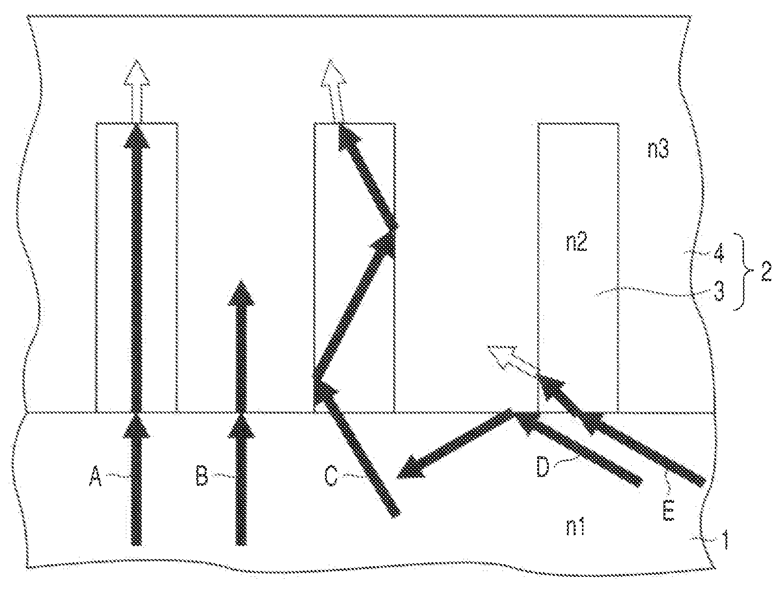
[0058]In a light-emitting diode shown in FIG. 8, an n-type GaN layer 12, an active layer 13, a p-type GaAlN layer (electron overflow prevention layer) 14, a first contact layer 15 made of a p-type GaN, and a second contact layer 16 made of a p-type GaN are sequentially formed on a substrate 11 made of GaN, SiC, or sapphire. Additionally, a p-type electrode layer 17 is formed on the second contact layer 16 made of the p-type GaN, and an n-type electrode layer 18 is formed on the n-type GaN layer 12.
[0059]The light-emitting diode of FIG. 8 is produced as follows.
[0060]First, the n-type GaN layer 12, in which an n-type impurity is doped, is formed on the substrate 11 by the crystal growth method. For example, metal organic chemical vapor deposition (MOCVD) can be used in the crystal growth method. In addition to MOCVD, molecular beam epitaxy (MBE) may be employed. Various elements such as Si and Ge can be used as the n-type impurity. In Example 1, Si is used as the n-type impurity. A S...
example 2
[0073]As shown in FIG. 11, in a structure of a light-emitting diode of Example 2, electrodes are provided at the top and bottom of the substrate interposed therebetween, such that current flows in a vertical direction.
[0074]In the light-emitting diode shown in FIG. 11, an n-type GaN layer 22, an active layer 23, a p-type GaAlN layer (electron overflow prevention layer) 24, a first contact layer 25 made of a p-type GaN, and a second contact layer 26 made of a p-type GaN are sequentially formed on an n-type GaN substrate 21. Additionally, a p-type electrode layer 27 is formed on the second contact layer 26 made of the p-type GaN, and an n-type electrode layer 28 is formed on the n-type GaN layer 21.
[0075]The light-emitting diode of FIG. 11 structured as described above is produced as follows.
[0076]First, the n-type GaN layer 22, in which the n-type impurity is doped, is formed on the n-type GaN substrate 21 by crystal growth method. For example, metal organic chemical vapor deposition...
example 3
[0091]As shown in FIG. 13, in a structure of a light-emitting diode of Example 3, a light is extracted through a transparent electrode.
[0092]In a light-emitting diode shown in FIG. 13, an n-type GaN layer 32, an active layer 33, a p-type GaAlN layer (electron overflow prevention layer) 34, a contact layer 35 made of a p-type GaN, and a transparent electrode 36 trough which a light emitted from the active layer 33 passes are sequentially formed on a substrate 31 made of GaN, SiC, or sapphire.
[0093]The light-emitting diode of FIG. 13 is manufactured as follows.
[0094]First, the n-type GaN layer 32, in which an n-type impurity is doped, is formed on the substrate 3 by a crystal growth method. For example, metal organic chemical vapor deposition (MOCVD) can be used as the crystal growth method. In addition to MOCVD, a molecular beam epitaxy (MBE) may be employed. Various elements such as Si and Ge can be used as the n-type impurity. In Example 3, Si is used as the n-type impurity.
[0095]N...
PUM
 Abstract
Description
Claims
Application Information
 - R&D Engineer
- R&D Manager
- IP Professional
- Industry Leading Data Capabilities
- Powerful AI technology
- Patent DNA Extraction
Browse by: Latest US Patents, China's latest patents, Technical Efficacy Thesaurus, Application Domain, Technology Topic, Popular Technical Reports.
© 2024 PatSnap. All rights reserved.Legal|Privacy policy|Modern Slavery Act Transparency Statement|Sitemap|About US| Contact US: help@patsnap.com