Insulating transformer and power conversion device

a technology of transformer and power conversion device, which is applied in the direction of transformer/inductance coil/winding/connection, electronic switching, pulse technique, etc., can solve the problems the difficulty of satisfying the demands of continuous operation for ten years or longer in high-temperature environments, and the occurrence of dielectric breakdown of the separation layer 59/b>, so as to improve reliability and environmental tolerance. , the effect of improving the toleran

Active Publication Date: 2009-02-26
FUJI ELECTRIC CO LTD
View PDF12 Cites 52 Cited by
  • Summary
  • Abstract
  • Description
  • Claims
  • Application Information

AI Technical Summary

Benefits of technology

[0086]By this means, while enabling miniaturization of insulating transformers using miniaturization machining techniques, an ESD tolerance voltage of 15 to 30 kV can be secured, the reliability of the insulating transformer can be secured, and the effect of noise arising from external magnetic flux can be alleviated, and signals can be exchanged while maintaining electrical insulation of the low-voltage side and high-voltage side. Hence, there is no longer need to use photocouplers, and environmental tolerance can be enhanced while suppressing the aging degradation.
[0087]As explained above, by means of this invention, an insulating transformer can be miniaturized using miniaturization machining techniques, the interval between the primary windings and secondary windings of the insulating transformer can be made several tens of μm or greater, the effect of noise arising from external magnetic flux can be alleviated while improving reliability and environmental tolerance, and signals can be exchanged while maintaining the electrical insulation of the low-voltage side and high-voltage side.

Problems solved by technology

And, when using a photocoupler as the insulated transmission means of an intelligent power module for the buck-boost converter of FIG. 9, circuit design must be performed while taking the above points into consideration, but it is difficult to satisfy demands for continuous operation of ten years or longer in high-temperature environments, such as those of vehicles or industrial equipment.
Therefore, there has been a problem that, if a voltage between 15 and 30 kV is applied to the separation layer 59, dielectric breakdown of the separation layer 59 occurs.

Method used


Image

  • Insulating transformer and power conversion device
  • Insulating transformer and power conversion device
  • Insulating transformer and power conversion device

Examples


first embodiment

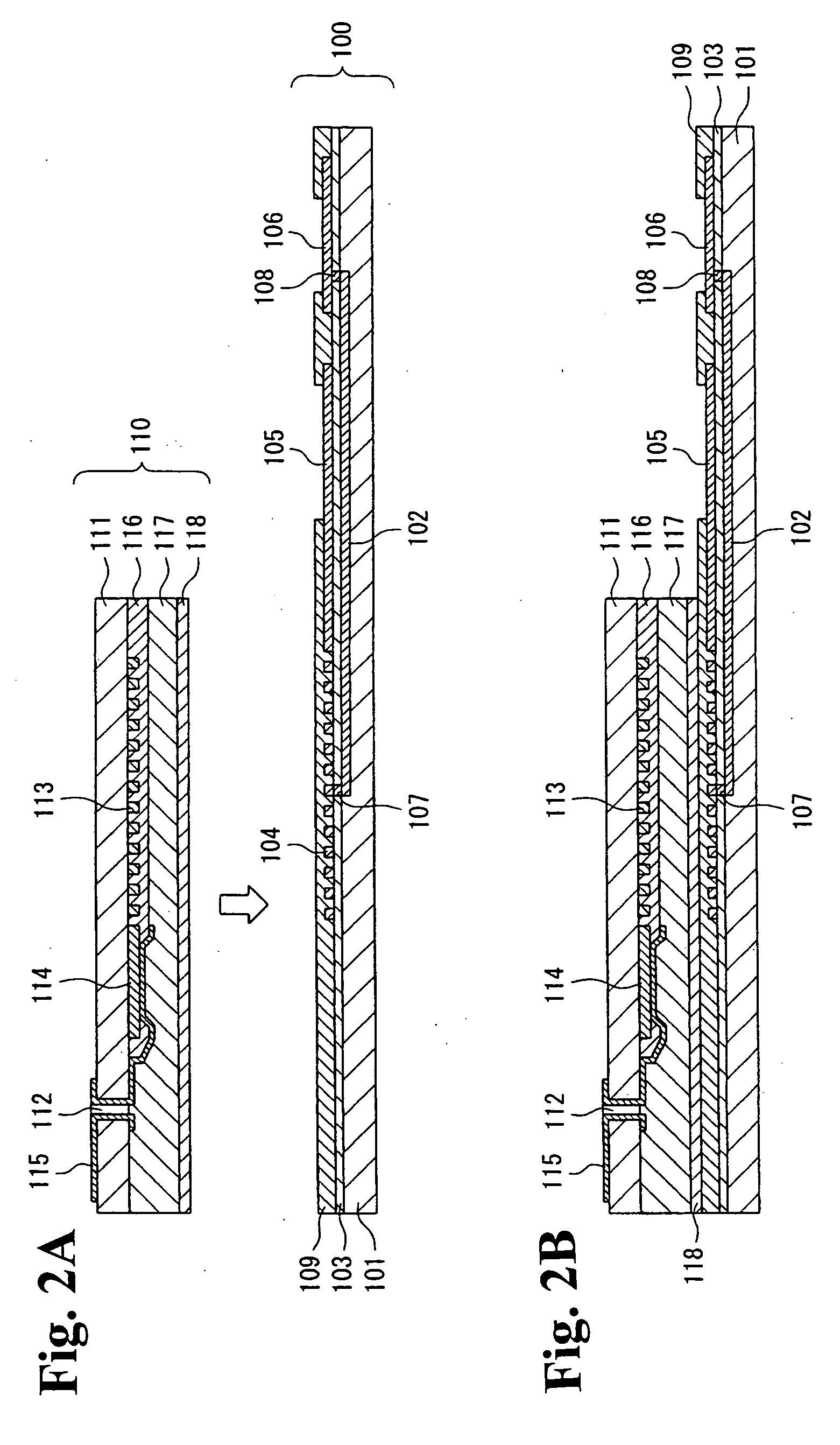
[0122]FIGS. 2A, 2B are cross-sectional views briefly showing the configuration of the insulating transformer of the invention.

[0123]In FIGS. 2A, 2B, the insulating transformer is provided with a primary-side coil 110, formed on an insulating substrate 111, and with a secondary-side coil 100, formed on a semiconductor substrate 101.

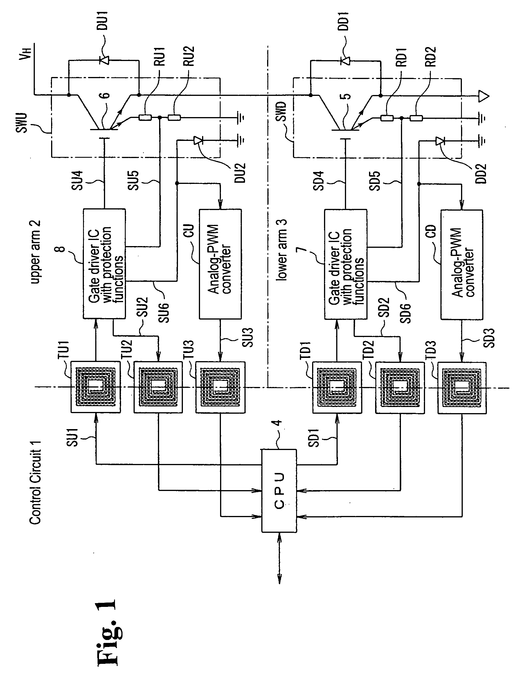
[0124]Here, in the secondary-side coil 100, a lead wire layer 102 is buried in the semiconductor substrate 101, and the secondary coil pattern 104 and electrodes patterns 105, 106 are formed on the semiconductor substrate 101, with an insulating layer 103 intervening. The gate driver ICs 7 and 8 with protection functions, analog-PWM converters CU and CD, and other integrated circuitry, or the switching elements SWU and SWD, and similar shown in FIG. 1 may be formed on the semiconductor substrate 101. The material of the semiconductor substrate 101 can, for example, be selected from among Si, Ge, SiGe, SiC, SiSn, PbS, GaAs, InP, GaP, GaN, ZnSe, or similar. ...

second embodiment

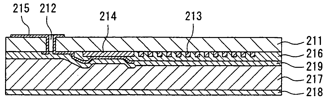
[0152]FIG. 5 is a cross-sectional view briefly showing the configuration of the primary-side coil of the insulating transformer of the invention.

[0153]In FIG. 5, a primary coil pattern 213 and electrode pattern 214 are formed on a first main face of an insulating substrate 211, and the primary coil pattern 213 and electrode pattern 214 are covered by an insulating layer 216 so as to expose the connection surface of the electrode pattern 214. As the insulating substrate 211, for example, a glass plate, ceramic substrate, resin substrate, or similar can be used. Alternatively, a Si substrate or other semiconductor substrate may be used. When the material of the insulating substrate 211 does not have insulating properties, an insulating layer may be formed on the surface so as to provide the substrate with insulating properties.

[0154]On the other hand, an electrode pattern 215 for wire extraction is formed on the second main face of the insulating substrate 211 opposite to the first ma...


PUM


Abstract

An insulating transformer includes a semiconductor substrate, an insulating substrate, a primary winding provided on one of the semiconductor substrate and the insulating substrate, a secondary winding provided on other of the semiconductor substrate and the insulating substrate, and an insulating spacer layer provided in between the semiconductor substrate and the insulating substrate for insulating and separating the primary winding and the secondary winding. The primary winding and the secondary winding are disposed to face each other. The insulating spacer layer maintains a constant interval between the semiconductor substrate and the insulating substrate.

Description

BACKGROUND OF THE INVENTION AND RELATED ART STATEMENT[0001]The present invention relates to an insulating transformer and a power conversion device, and more specifically to an insulating transformer suitable for an application of a method employing glass substrate for the insulation of the primary-side windings and the secondary-side windings of the insulating transformer.[0002]In recent years, in order to provide automotive equipments with higher efficiencies and reduced power consumptions, buck-boost converters and inverters have been provided in driving systems for electric motors which generate driving force.[0003]FIG. 6 is a block diagram roughly showing the configuration of an automotive driving system using a conventional buck-boost converter.[0004]In FIG. 6, the automotive driving system comprises a power supply 1101, which supplies power to the buck-boost converter 1102; the buck-boost converter 1102, which raises and lowers voltages; an inverter 1103, which converts a vol...

Claims


Application Information

Patent Timeline
Patent Type & Authority Applications(United States)
IPC IPC(8): H02M7/00
CPCH01F27/2804H01F27/323H03K17/0828H03K2017/0806H03K17/567H03K17/691H03K17/18
Inventor EDO, MASAHARUUENO, KATSUNORIYOSHIMURA, HIROYUKI
Owner FUJI ELECTRIC CO LTD
Why Eureka
Try Eureka