Micro and NANO structures in an elastomeric material

a technology of elastomeric materials and nano-structures, applied in vacuum evaporation coatings, sputtering coatings, photographic processes, etc., can solve the problems of limited use of sl patterning techniques and cannot be patterned using conventional lithographic methods, and achieves high time consumption, large cost, and easy to use

Inactive Publication Date: 2009-02-26
FORSKARPATENT I LINKOPING
View PDF3 Cites 19 Cited by
  • Summary
  • Abstract
  • Description
  • Claims
  • Application Information

AI Technical Summary

Benefits of technology

[0017]The invention is therefore related to the need for bridging the microscale and the nanoscale. Simultaneous and easy exploitation of structures at both the microscale and nanoscale has so far been hindered by large cost and relatively high time consumption. Elastomers and soft lithographic patterning techniques have here been identified as candidates for solving this problem in a cheap and easy way. The clear advantage of elasticity often emphasized in soft lithography, is however also an inherent limitation when it comes to working with features that are very different in size. The probability for material collapsing and sagging is high if considerations are not taken. The crucial limitations of elastomeric materials are therefore identified and solved with the introduction of a material dependent “dynamic working range”. By always maintaining any aspect ratio of any elastomer structure within the dynamic working range, any possibility for simultaneous exploitation of both micro structures and nano structures is open.

Problems solved by technology

There are numerous materials with properties that are interesting at supermicrometer, micrometer and submicrometer sizes, but that can not be patterned using conventional lithographic methods.
The sagging (608) of elastomers caused by compressive forces between the stamp and the substrate limits the use of most SL patterning techniques.

Method used


Image

  • Micro and NANO structures in an elastomeric material
  • Micro and NANO structures in an elastomeric material
  • Micro and NANO structures in an elastomeric material

Examples


example 1

Molding of Template

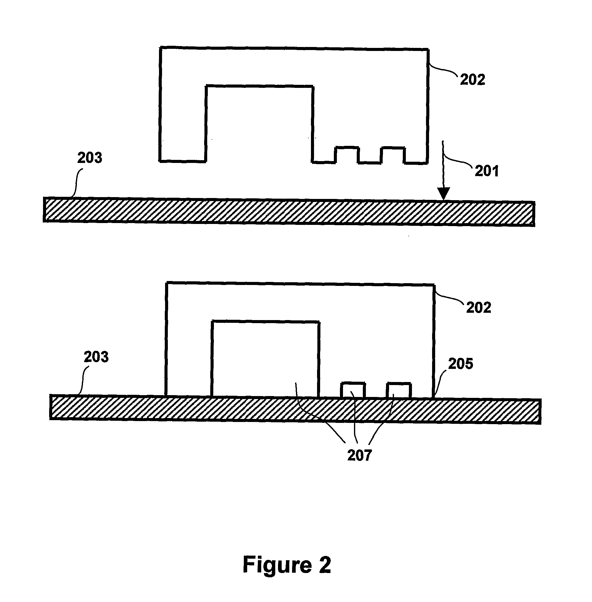
[0071]Sylgard 184 (Dow Corning, UK), a two component silicone rubber (poly(dimethylsiloxane), PDMS), is used to prepare elastomeric device from the micro-nano SU-8 template, that is depicted in FIG. 3. and FIG. 5.

[0072]The prepolymer and the curing agent are mixed according to the instructions provided by the manufacturer. This is then poured on the SU-8 template and curing is accomplished by heating up to 130° C. for at least 20 min, but lower temperatures and longer incubation times can also be used depending requirements of stamp softness. Other stamp materials can also be used in the patterning step. The stamp is removed from the template after curing, and an inverted relief structure of the template is created in the elastomeric device.

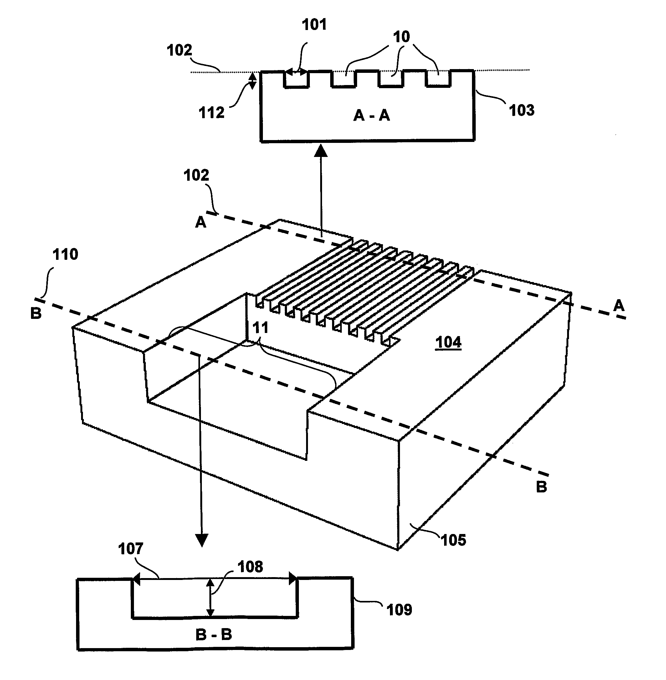
[0073]FIG. 1 illustrates schematically an elastomer device that is molded from the SU-8 template.

example 2

One Step Contact Printing

[0074]Using of elastomeric device for one step contact printing of nano structures that are separated by micrometers. This would not be possible without using the present invention since the micro space between the nano structures would sag.

example 3

Dye Lasers

[0075]Formation of channel structures for micro and nano fluidics, in which liquids that carry luminescent molecules and polymers, are distributed through the channels under steady flow conditions. Such structures may include micro patterned dye lasers, in which the dye solution is distributed into a micro patterned optical cavity, and constantly replenished with fresh solution as the dye is consumed under operation. Distributed Bragg reflectors would be implemented in the same mask, through nanostructures, which could operate on the reflection at an air / template or solution / template interface. Periodic submicron structures could also be used for in coupling and out coupling of light from an optical waveguide defined with the help of liquid in the channel.


PUM

PropertyMeasurementUnit
sizeaaaaaaaaaa
sizeaaaaaaaaaa
sizeaaaaaaaaaa

Abstract

The invention relates to an elastomeric device (105), wherein the elastomeric device contains a relief structure with indentations with respect to the base (110), (102) and wherein selected ones of said indentations comprise at least two indentation depths (112), (108) and indentation widths (101), (107). It also relates to a method of making a master for construction of said elastomeric device comprising a procedure to provide a pattern on a substrate of a suitable material. One step in. the construction of said elastomeric device comprises a molding procedure of an elastomer. Methods of using the elastomeric device in printing, fluidic control, sorting, lab-on-a-chip devices are also disclosed.

Description

FIELD OF THE INVENTION[0001]The present invention relates generally to soft lithographical patterning methods, and more specifically to generation of simultaneous and seamless supermicrometer and submicrometer structures in elastomeric materials. The present invention also relates to a method for construction of such structures in elastomeric materials.BACKGROUND OF THE INVENTION[0002]The development of nanotechnology requires efficient ways for fabrication of micron and submicron structures on the same substrate. In many applications, it is desired to fabricate micro and nano structures that are connected.[0003]One of the advantages of connected micro-nano structures is that micron structures can easily be addressed electrically, optically and mechanically allowing further addressing of the nano structures. There is also a great need for mechanical micro-nano structures, interfaces, definers, bridges that can be used on both planar and non-planar substrates.[0004]There are numerous...

Claims


Application Information

Patent Timeline
Patent Type & Authority Applications(United States)
IPC IPC(8): B32B5/00G03F7/20C23F1/02B28B11/08
CPCB01L3/5027B01L3/502707B01L2200/12B01L2300/0816B01L2300/0896B01L2300/123Y10T436/2575B82Y30/00B82Y40/00G03F7/0002G03F7/0017Y10T428/24479B82Y10/00Y10T137/2224
Inventor HAMEDI, MAHIARTVINGSTEDT, KRISTOFERASBERG, PETERINGANAS, OLLE
Owner FORSKARPATENT I LINKOPING
Why Eureka
Try Eureka