Method for fabricating capacitor in semiconductor device

Inactive Publication Date: 2009-03-05
SK HYNIX INC
View PDF4 Cites 4 Cited by
  • Summary
  • Abstract
  • Description
  • Claims
  • Application Information

AI Technical Summary

Benefits of technology

[0008]In this invention, when a capacitor is fabricated using a Ru layer, an adhesion strength of the Ru laye

Problems solved by technology

Furthermore, it is difficult to acquire precise electric characteristics from the capacitor due to an electric current change caused by an asymmetrical electric current-voltage characteristic of the MIS-structured capacitor.
However, when the Ru layer is formed through the ALD

Method used


Image

  • Method for fabricating capacitor in semiconductor device
  • Method for fabricating capacitor in semiconductor device
  • Method for fabricating capacitor in semiconductor device

Examples


Example

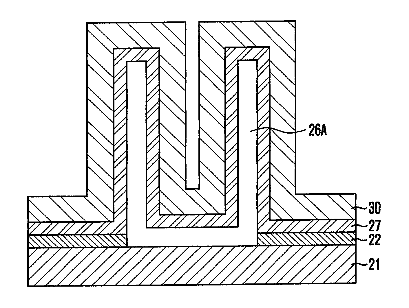
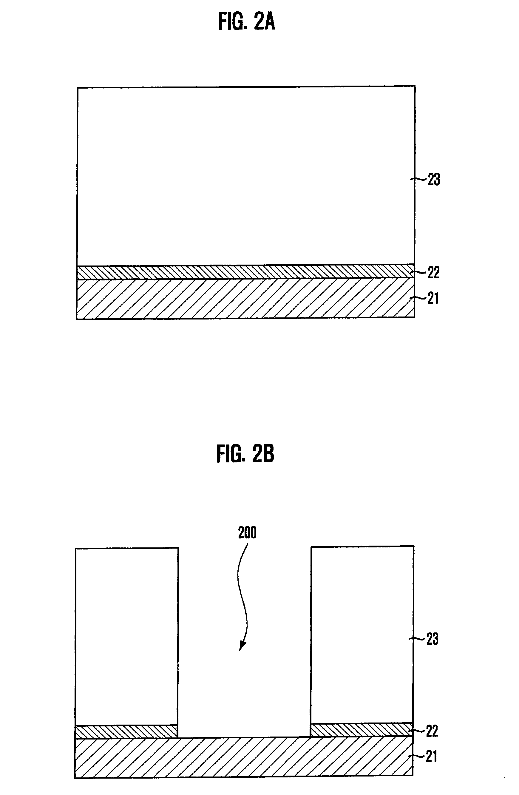
[0013]Embodiments of the present invention relate to a method for fabricating a capacitor in a semiconductor device.

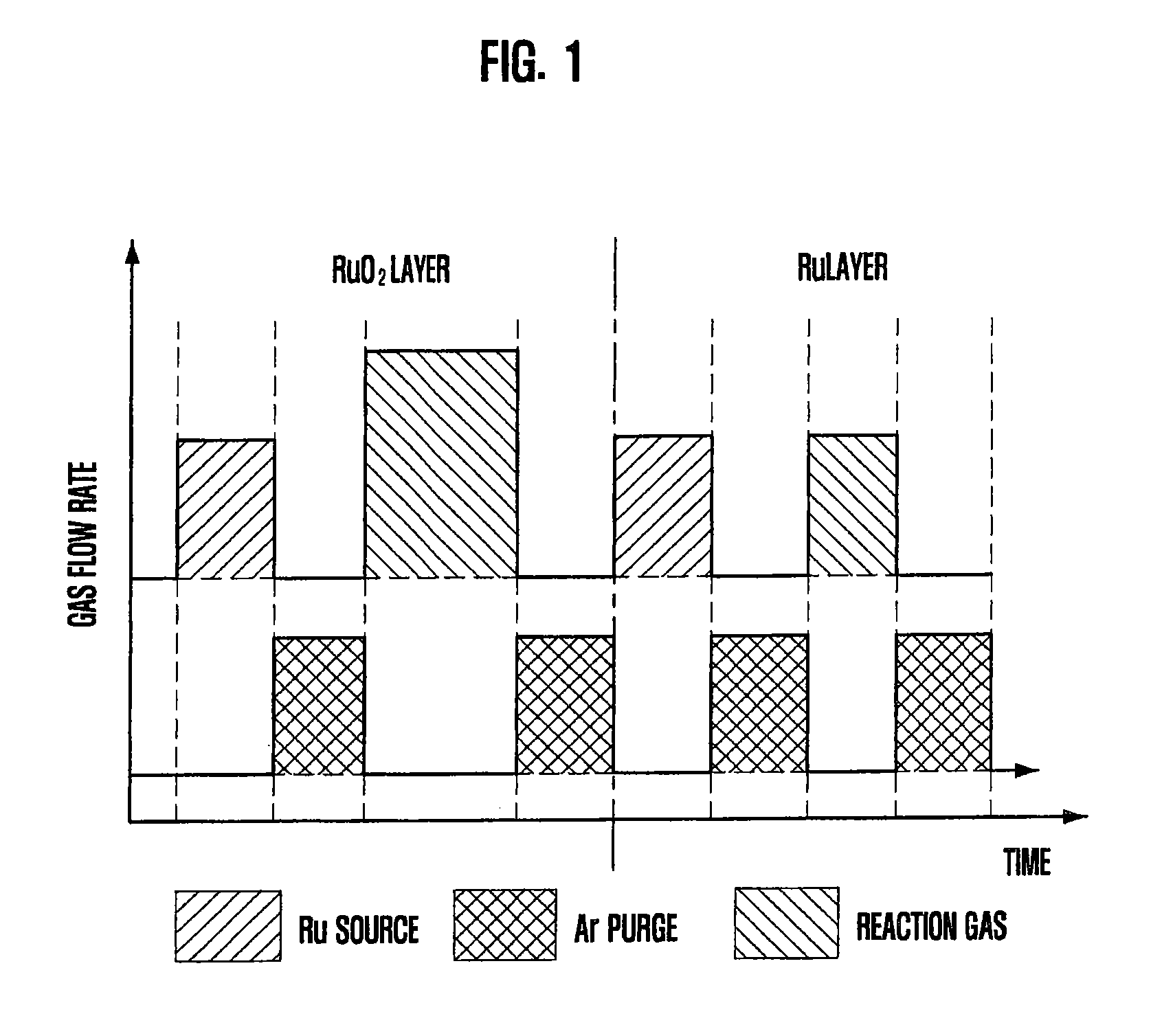
[0014]FIG. 1 is a graph describing a method for forming a RuO2 layer and a Ru layer through an ALD process.

[0015]Referring to FIG. 1, a RuO2 layer and Ru layer are formed through the ALD method including four processes. In a first process, a Ru source is implanted into a reaction chamber. In a second process, the reaction chamber is purged with argon (Ar) gas or nitrogen (N2) gas. In a third process, a reaction gas including oxygen (O2) or ozone (O3) is implanted (or supplied to provided) into the reaction chamber. In the fourth process, the reaction chamber is purged with the Ar gas or N2 gas to remove the gas that is not used in the reaction.

[0016]Flow rate of the reaction gas or implanting time may change. That is, when the Ru layer is formed, the flow rate or implanting time of the reaction gas is controlled to be under a certain value to form the Ru layer not cont...


PUM


Abstract

A method for fabricating a capacitor includes providing a substrate having a capacitor region is employed, forming a first Ru1-xOx layer over the substrate, forming a Ru layer for a lower electrode over the first Ru1-xOx layer and deoxidizing the first Ru1-xOx layer, forming a dielectric layer over the Ru layer for a lower electrode, and forming a conductive layer for an upper electrode over the dielectric layer, wherein the first Ru1-xOx layer contains oxygen in an amount less than an oxygen amount of a RuO2 layer.

Description

CROSS-REFERENCE TO RELATED APPLICATIONS[0001]The present invention claims priority of Korean patent application number 2007-0088047, filed on Aug. 31, 2007, which is incorporated by reference in its entirety.BACKGROUND OF THE INVENTION[0002]The present invention relates to a method for fabricating a semiconductor device, and more particularly, to a method for fabricating a capacitor using a metal layer, e.g., a ruthenium (Ru) layer, as a lower electrode or an upper electrode in a semiconductor device.[0003]Generally, a capacitor in a memory cell includes a lower electrode for a storage, a dielectric layer, and an upper electrode for a plate. To acquire a large capacitance within limited dimensions, it is required to secure a thin dielectric layer, decrease effective dimensions by forming a three-dimensional capacitor, or apply a dielectric layer with a high permittivity such as a tantalum pentoxide (Ta2O5) layer.[0004]When the Ta2O5 layer is used as a dielectric layer in a capacitor...

Claims


Application Information

Patent Timeline
IPC IPC(8): H01L21/02
CPCH01L28/75H01L28/65H01L21/20H10B12/00
Inventor DO, KWAN-WOOROH, JAE-SUNGLEE, KEE-JEUNGKIL, DEOK-SINKIMKIM, JIN-HYOCKPARK, KYUNG-WOONG
Owner SK HYNIX INC
Why Eureka
Try Eureka